

Form 6-K ASML HOLDING NV For: Nov 24
 Tweet
Tweet Share
Share�
�
SECURITIES AND EXCHANGE COMMISSION
Washington, D.C. 20549
�
�
FORM 6-K
�
�
REPORT OF A FOREIGN ISSUER
PURSUANT TO RULE 13A-16 OR 15D-16
OF THE SECURITIES EXCHANGE ACT OF 1934
For November�24, 2014
�
�
ASML Holding N.V.
�
�
De Run 6501
5504 DR Veldhoven
The Netherlands
(Address of principal executive offices)
�
�
Indicate by check mark whether the registrant files or will file annual reports under cover of Form 20-F or Form 40-F.
Form 20-F��x������������Form 40-F���
Indicate by check mark whether the registrant by furnishing the information contained in this Form is also thereby furnishing the information to the Commission pursuant to Rule 12g3-2(b) under the Securities Exchange Act of 1934.
Yes���������������No� �x
If �Yes� is marked, indicate below the file number assigned to the registrant in connection with Rule 12g3-2(b):������������
�
�
�

�
| Exhibits |
�� | � |
| 99.1 | �� | �ASML Outlines Long-Term Growth Opportunity at Investor Day; Receives First Order for EUV Production Systems�, press release date November 24, 2014 |
| 99.2 | �� | �Creating value for all stakeholders�, presentation dated November 24, 2014 |
| 99.3 | �� | �Many ways to shrink: The right moves to 10 nanometer and beyond�, presentation dated November�24, 2014 |
| 99.4 | �� | �DUV�, presentation dated November 24, 2014 |
| 99.5 | �� | �Holistic Lithography�, presentation dated November 24, 2014 |
| 99.6 | �� | �EUV�, presentation dated November 24, 2014 |
| 99.7 | �� | �Market Update�, presentation dated November 24, 2014 |
| 99.8 | �� | �Financial Model�, presentation dated November 24, 2014 |
| 99.9 | �� | �Closing Remarks�, presentation dated November 24, 2014 |
SIGNATURES
Pursuant to the requirements of the Securities Exchange Act of 1934, the registrant has duly caused this report to be signed on its behalf by the undersigned, thereunto duly authorized.
�
| � | � | ASML HOLDING N.V. (Registrant) | ||||
| Date: November�24, 2014 | � | � | By: | � | /s/ Peter T.F.M. Wennink | |
| � | � | � | Peter T.F.M. Wennink | |||
| � | � | � | Chief Executive Officer | |||
Exhibit 99.1
�
�
ASML Outlines Long-Term Growth Opportunity at Investor Day; Receives First Order for EUV Production Systems
LONDON, 24�November 2014 - At its Investor Day, ASML Holding N.V. (ASML) will today outline its expected opportunity to grow net sales to about EUR 10 billion and to triple earnings per share by 2020.
ASML also announces that Taiwan Semiconductor Manufacturing Company Ltd. (TSMC) has ordered two NXE:3350B EUV systems for delivery in 2015 with the intention to use those systems in production. In addition, two NXE:3300B systems already delivered to TSMC will be upgraded to NXE:3350B performance.
ASML�s executive management will present the 2020 ambition in more detail from 13:00 GMT (14:00 CET) at the Investor Day in London. The presentations will also be webcast live at www.asml.com.
Underpinning ASML�s 2020 ambition is the semiconductor industry�s continued aggressive pursuit of transistor scaling to deliver improvements in performance, size and power consumption, which in turn makes possible new applications and more attractive consumer devices and services, fuelling overall industry growth. In short, ASML expects Moore�s Law to continue to drive the industry in the coming ten years, with lithography as the key enabler.
Regarding our main technologies, we expect
Deep-UV immersion systems to be used for patterning of multiple layers in all advanced processes for the forseeable future;
EUV to enable cost effective manufacturing of logic, DRAM and NAND chips from 2016/2017 allowing feature size shrink and simplification of manufacturing processes;
Holistic Lithography products to deliver advanced correction capability supporting the tightening of litho related manufacturing tolerances, resulting in lower rework and higher yields.
About ASML ASML makes possible affordable microelectronics that improve the quality of life. ASML invents and develops complex technology for high-tech lithography machines for the semiconductor industry. ASML�s guiding principle is continuing Moore�s Law towards ever smaller, cheaper, more powerful and energy-efficient semiconductors. Our success is based on three pillars: technology leadership combined with customer and supplier intimacy, highly efficient processes and entrepreneurial people. We are a multinational company with over 70 locations in 16 countries, headquartered in Veldhoven, the Netherlands. We employ more than 13,800 people on payroll and flexible contracts (expressed in full time equivalents). Our company is an inspiring place where employees work, meet, learn and share. ASML is traded on Euronext Amsterdam and NASDAQ under the symbol ASML. More information about ASML, our products and technology, and career opportunities is available on: www.asml.com
Forward Looking Statements This document contains statements relating to certain projections and business trends that are forward-looking, including statements with respect to our outlook, expected customer demand in specified market segments, expected sales levels and trends, our market share, customer orders and systems backlog, IC unit demand, expected or indicative financial results or targets, including revenue, gross margin, expenses, gross margin percentage, opex percentage of sales, tax percentage, cash conversion cycle, capex percentage of sales, credit rating and earnings per share, expected shipments of tools and the timing thereof, including expected shipments of EUV and DUV tools, productivity of our tools and systems performance, including EUV system performance (such as endurance tests), the development of EUV technology and timing of shipments, development in IC technology, including shrink scenarios, NAND technology development and cost estimates, expectations on development of the shrink roadmap across all of our systems, upgradeability of
ASML
Page 1 of 3
�
our tools, system and upgrade orders, customer transition estimates, expected transition scaling, forecasted industry developments, including expected smartphone, tablet and server use in future years, and expectations relating to new applications including wearable devices and connected devices, expected investment pay-back time for foundries, expected construction of additional holistic lithography infrastructure, the continuation of Moore�s Law, and our dividend policy and intention to repurchase shares. You can generally identify these statements by the use of words like �may�, �will�, �could�, �should�, �project�, �believe�, �anticipate�, �expect�, �plan�, �estimate�, �forecast�, �potential�, �intend�, �continue� and variations of these words or comparable words. These statements are not historical facts, but rather are based on current expectations, estimates, assumptions and projections about the business and our future financial results and readers should not place undue reliance on them.
Forward-looking statements do not guarantee future performance and involve risks and uncertainties. These risks and uncertainties include, without limitation, economic conditions, product demand and semiconductor equipment industry capacity, worldwide demand and manufacturing capacity utilization for semiconductors (the principal product of our customer base), the impact of general economic conditions on consumer confidence and demand for our customers� products, competitive products and pricing, affordability of shrink, the continuation of Moore�s Law, the impact of manufacturing efficiencies and capacity constraints, performance of our systems, the continuing success of technology advances and the related pace of new product development and customer acceptance of new products and customers meeting their own development roadmaps, market demand for our existing products and for new products and our ability to maintain or increase or market share, the development of and customer demand for multi-patterning technology and our ability to meet overlay and patterning requirements, the number and timing of EUV systems expected to be shipped, our ability to enforce patents and protect intellectual property rights, the risk of intellectual property litigation, EUV system performance and customer acceptance, availability of raw materials and critical manufacturing equipment, trade environment, our ability to reduce costs, changes in exchange rates and tax rates, available cash, distributable reserves for dividend payments and share repurchases, changes in our treasury policy, including our dividend and repurchase policy, failure to complete orders, including due to failure to meet purchase order performance conditions (for new systems and upgrades), the risk that key assumptions underlying financial targets prove inaccurate, including assumptions relating to market share, lithography market growth and our customers� ability to reduce productions costs, risks associated with Cymer, which we acquired in 2013, and other risks indicated in the risk factors included in ASML�s Annual Report on Form 20-F and other filings with the US Securities and Exchange Commission. These forward-looking statements are made only as of the date of this document. We do not undertake to update or revise the forward-looking statements, whether as a result of new information, future events or otherwise.
Lucas van Grinsven
Communication Worldwide | Corporate
+316 101 99 532
Niclas Mika
Corporate Communications
+31 6 201 528 63
Craig DeYoung
VP Investor Relations Worldwide
+1.480.696.2762
Page 2 of 3
ASML

�
Marcel Kemp
Director Investor Relations - Europe
+31.40.268.6494
Copyright 2012 (ASML) All rights reserved
ASML.com > Press > Press Releases > ASML Outlines Long-Term Growth...
ASML
Page 3 of 3
Exhibit 99.2
�
�
ASML
Creating value for all stakeholders
Peter Wennink
President & Chief Executive Officer
24 November 2014
INVESTOR DAY
ASMLSMALLTALK2014
LONDON
�
Forward looking statements
ASML
Public
Slide 2
November 2014
This document contains statements relating to certain projections and business trends that are forward-looking, including statements with respect to our outlook, expected customer demand in specified market segments, expected sales levels and trends, our market share, customer orders and systems backlog, IC unit demand, expected or indicative financial results or targets, including revenue, gross margin, expenses, gross margin percentage, opex percentage of sales, tax percentage, cash conversion cycle, capex percentage of sales, credit rating and earnings per share, expected shipments of tools and the timing thereof, including expected shipments of EUV and DUV tools, productivity of our tools and systems performance, including EUV system performance (such as endurance tests), the development of EUV technology and timing of shipments, development in IC technology, including shrink scenarios, NAND technology development and cost estimates, expectations on development of the shrink roadmap across all of our systems, upgradeability of our tools, system orders, customer transition estimates, expected transition scaling, forecasted industry developments, including expected smartphone, tablet and server use in future years, and expectations relating to new applications including wearable devices and connected devices, expected investment pay-back time for foundries, expected construction of additional holistic lithography infrastructure, the continuation of Moore�s Law, and our dividend policy and intention to repurchase shares. You can generally identify these statements by the use of words like �may�, �will�, �could�, �should�, �project�, �believe�, �anticipate�, �expect�, �plan�, �estimate�, �forecast�, �potential�, �intend�, �continue� and variations of these words or comparable words. These statements are not historical facts, but rather are based on current expectations, estimates, assumptions and projections about the business and our future financial results and readers should not place undue reliance on them.
Forward-looking statements do not guarantee future performance and involve risks and uncertainties. These risks and uncertainties include, without limitation, economic conditions, product demand and semiconductor equipment industry capacity, worldwide demand and manufacturing capacity utilization for semiconductors (the principal product of our customer base), the impact of general economic conditions on consumer confidence and demand for our customers� products, competitive products and pricing, affordability of shrink, the continuation of Moore�s Law, the impact of manufacturing efficiencies and capacity constraints, performance of our systems, the continuing success of technology advances and the related pace of new product development and customer acceptance of new products and customers meeting their own development roadmaps, market demand for our existing products and for new products and our ability to maintain or increase or market share, the development of and customer demand for multi-patterning technology and our ability to meet overlay and patterning requirements, the number and timing of EUV systems expected to be shipped, our ability to enforce patents and protect intellectual property rights, the risk of intellectual property litigation, EUV system performance and customer acceptance, availability of raw materials and critical manufacturing equipment, trade environment, our ability to reduce costs, changes in exchange rates and tax rates, available cash, distributable reserves for dividend payments and share repurchases, changes in our treasury policy, including our dividend and repurchase policy, completion of sales orders, the risk that key assumptions underlying financial targets prove inaccurate, including assumptions relating to market share, lithography market growth and our customers� ability to reduce productions costs, risks associated with Cymer, which we acquired in 2013, and other risks indicated in the risk factors included in ASML�s Annual Report on Form 20-F and other filings with the US Securities and Exchange Commission. These forward-looking statements are made only as of the date of this document. We do not undertake to update or revise the forward-looking statements, whether as a result of new information, future events or otherwise.

�
Summary: ASML�s positioning, opportunities and threats
ASML
Public
Slide 3
November 2014
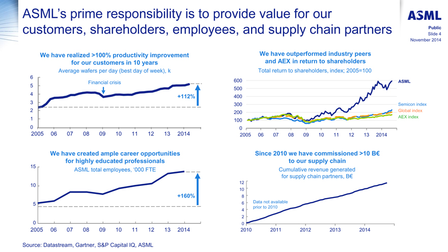
ASML�s prime responsibility is to provide value for our customers, shareholders, employees, and supply chain partners
Our success is based on delivering Litho products with superior performance at lowest cost of ownership and on our flexible operating model required for an inherently volatile market
ASML models an annual total revenue opportunity of 10B€ by 2020 and subsequent growth beyond
We have reviewed our most impactful threats and feel confident about our approach to mitigate these
�
ASML�s prime responsibility is to provide value for our customers, shareholders, employees, and supply chain partners
ASML
Public
Slide 4
November 2014
We have realized >100% productivity improvement
for our customers in 10 years
Average wafers per day (best day of week), k
6
5
4
3
2
1
0
2005 06
Financial crisis
07
08
09
10
11
12
+112%
13 2014
600
500
400
300
200
100
0
2005
We have outperformed industry peers
and AEX in return to shareholders
Total return to shareholders, index; 2005=100
06
07
08
09
10
11
12
13
2014
ASML
Semicon index
Global index
AEX index
15
10
5
0
2005
We have created ample career opportunities
for highly educated professionals
ASML total employees, �000 FTE
06
07
08
09
10
11
12
+160%
13 2014
12
10
8
6
4
2
0
2010
Since 2010 we have commissioned >10 B€
to our supply chain
Cumulative revenue generated
for supply chain partners, B€
Data not available
prior to 2010
2011
2012
2013
2014
Source: Datastream, Gartner, S&P Capital IQ, ASML
�
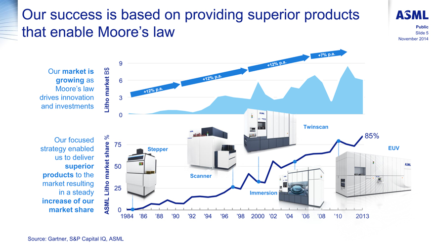
Our success is based on providing superior products that enable Moore�s law
ASML
Public
Slide 5
November 2014
Our market is growing as Moore�s law drives innovation and investments
Litho market B$
9
6
3
+12% p.a.
+12% p.a.
+12% p.a.
+7% p.a.
0
Our focused strategy enabled us to deliver superior products to the market resulting in a steady increase of our market share
ASML Litho market share %
75
Stepper
Scanner
Immersion
Twinscan
EUV
85%
50
25
0
1984
�86
�88
�90
�92
�94
�96
�98
�2000
�02
�04
�06
�08
�10
2013
Source: Gartner, S&P Capital IQ, ASML
�
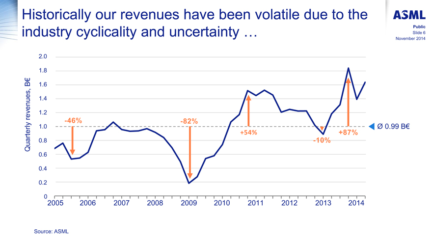
Historically our revenues have been volatile due to the industry cyclicality and uncertainty...
ASML
Public
Slide 6
November 2014
Quarterly revenues, B€
2.0
1.8
1.6
1.4
1.2
-46%
-82%
1.0
�0.99 B€
+54%
+87%
0.8
-10%
0.6
0.4
0.2
0
2005
2006
2007
2008
2009
2010
2011
2012
2013
2014
Source: ASML
�
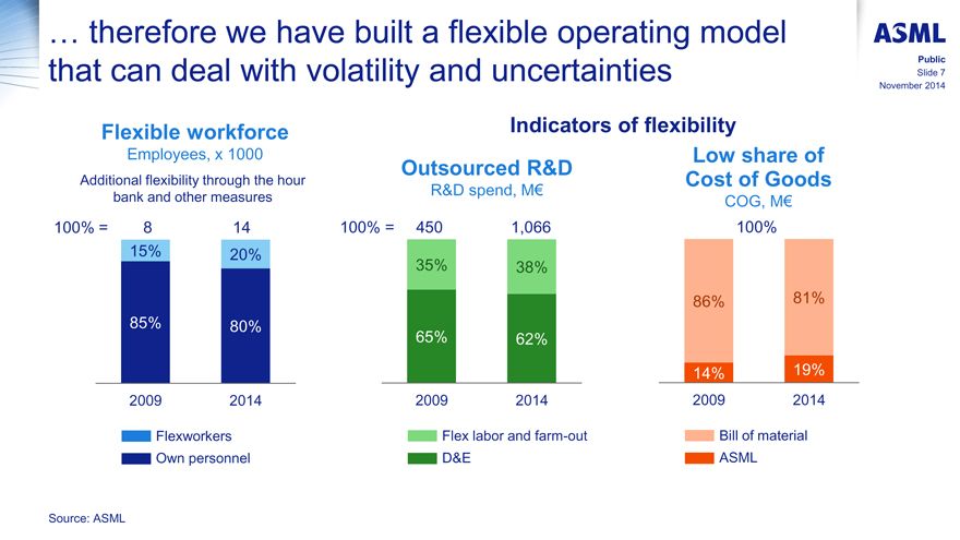
... therefore we have built a flexible operating model that can deal with volatility and uncertainties
ASML
Public
Slide 7
November 2014
Flexible workforce
Indicators of flexibility
Employees, x 1000
Low share of
Additional flexibility through the hour bank and other measures
Outsourced R&D
Cost of Goods
R&D spend, M€
COG, M€
100% =8
14
100% =
450
1,066
100%
15%
20%
86%
81%
35%
38%
85%
80%
65%
62%
14%
19%
2009
2014
2009
2014
2009
2014
Flexworkers
Flex labor and farm-out
Bill of material
Own personnel
D&E
ASML
Source: ASML
�
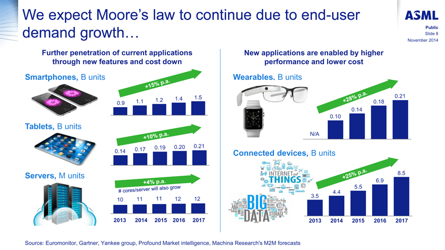
We expect Moore�s law to continue due to end-user demand growth...
ASML
Public
Slide 8
November 2014
Further penetration of current applications
New applications are enabled by higher
through new features and cost down
performance and lower cost
Smartphones, B units
Wearables, B units
+28% p.a.
+15% p.a.
0.21
0.9
1.1
1.2
1.4
1. 5
0.18
0.14
0.10
Tablets, B units
N/A
+10% p.a.
0.14
0.17
0.19
0.20
0.21
Connected devices, B units
Servers, M units
Internet of things
+25% p.a.
8.5
+4% p.a.
Big Data
6.9
# cores /server will also grow
5.5
4.4
10
11
11
12
12
3.5
2013
2014
2015
2016
2017
2013
2014
2015
2016
2017
Source: Euromonitor, Gartner, Yankee group, Profound Market intelligence, Machina Research�s M2M forecasts
�
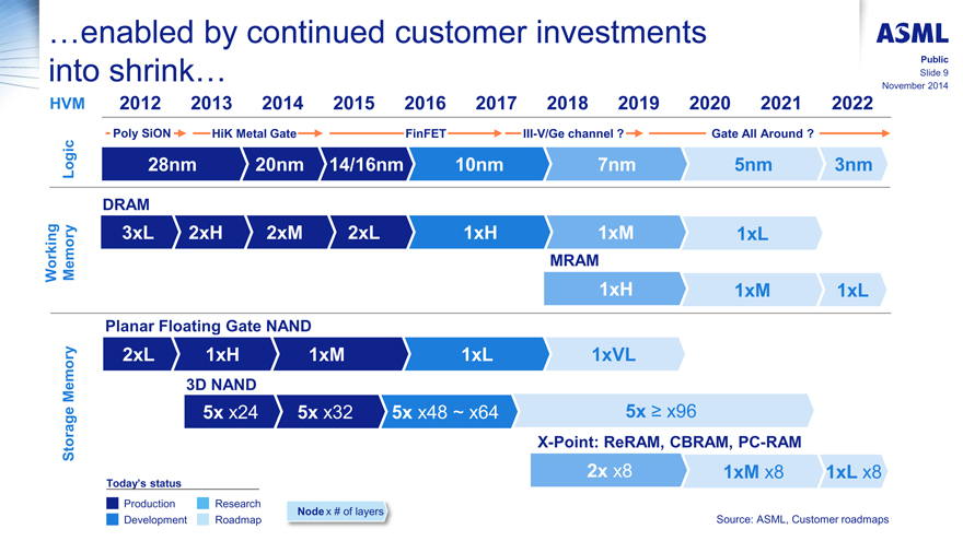
�enabled by continued customer investments into shrink
ASML Public Slide 9 November 2014
HVM 2012 2013 2014 2015 2016 2017 2018 2019 2020 2021 2022
Logic Poly SiON HiK Metal Gate FinFET III-V/Ge channel ? Gate All Around ?
28nm 20nm 14/16nm 10nm 7nm 5nm 3nm
DRAM Working Memory 3xL 2xH 2xM 2xL 1xH 1xM 1xL
MRAM 1xH 1xM 1xL
Planar Floating Gate NAND Storage Memory 2xL 1xH 1xM 1xL 1xVL
3D NAND 5x x24 5x x32 5x x48 ~ x64 5x � x96
X-Point: ReRAM, CBRAM, PC-RAM 2x x8 1xM x8 1xL x8
Today�s status
Production Development
Research Roadmap
Node x # of layers
Source: ASML, Customer roadmaps
�
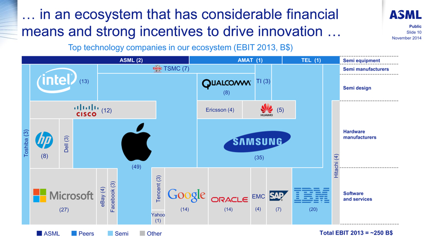
� in an ecosystem that has considerable financial means and strong incentives to drive innovation �
ASML Public Slide 10 November 2014
Top technology companies in our ecosystem (EBIT 2013, B$)
ASML (2) AMAT (1) TEL (1)
intel (13) TSMC (7)
Toshiba (3)
QUALCOMM� (8) TI (3) CISCO (12) Ericsson (4) HUAWEI (5) hp (8) Dell (3)
(49) SAMSUNG (35) Hitachi (4) Microsoft (27) eBay (4) Facebook (3) Tencent (3) Yahoo (1) Google (14) ORACLE (14)
EMC (4) SAP� (7) IBM (20)
Semi equipment
Semi manufacturers Semi design
Hardware manufacturers
Software and services
ASML Peers Semi Other
Total EBIT 2013 = ~250 B$
�
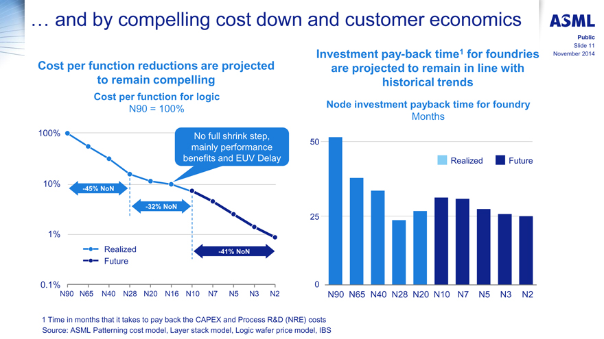
� and by compelling cost down and customer economics ASML Public Slide 11 November 2014
Cost per function reductions are projected to remain compelling
Cost per function for logic N90 = 100%
100% 10% 1% 0.1%
No full shrink step, mainly performance benefits and EUV Delay
-45% NoN -32% NoN -41% NoN
Realized
Future
N90 N65 N40 N28 N20 N16 N10 N7 N5 N3 N2
Investment pay-back time1 for foundries are projected to remain in line with historical trends
Node investment payback time for foundry
Months
50 25 0
Realized
Future
N90 N65 N40 N28 N20 N10 N7 N5 N3 N2
1 Time in months that it takes to pay back the CAPEX and Process R&D (NRE) costs
Source: ASML Patterning cost model, Layer stack model, Logic wafer price model, IBS
�
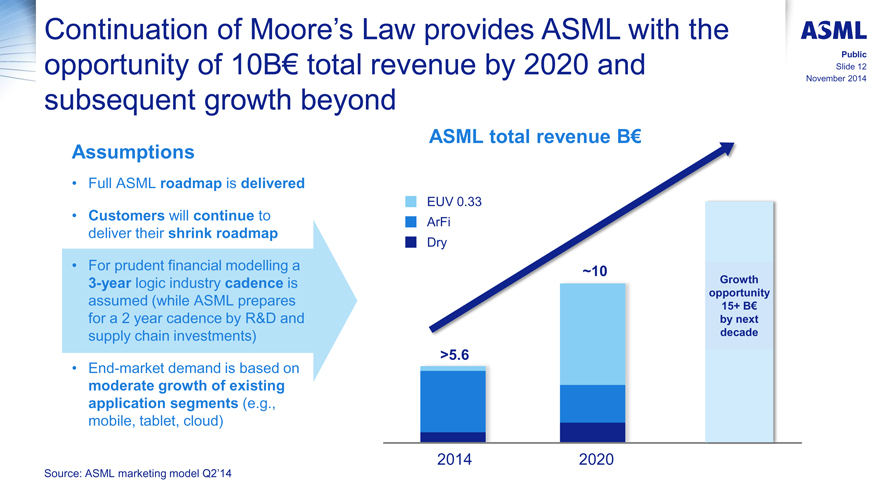
Continuation of Moore�s Law provides ASML with the opportunity of 10B€ total revenue by 2020 and subsequent growth beyond
ASML Public Slide 12 November 2014
Assumptions
Full ASML roadmap is delivered
Customers will continue to deliver their shrink roadmap
For prudent financial modelling a 3-year logic industry cadence is assumed (while ASML prepares for a 2 year cadence by R&D and supply chain investments)
End-market demand is based on moderate growth of existing application segments (e.g., mobile, tablet, cloud)
ASML total revenue B€
EUV 0.33
ArFi
Dry
>5.6
~10
Growth opportunity 15+ B€ by next decade
2014 2020
Source: ASML marketing model Q2�14
�
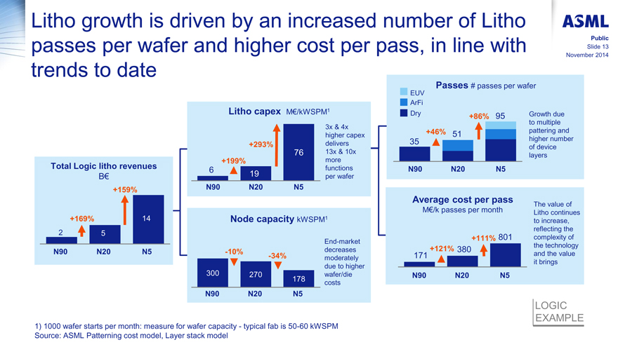
Litho growth is driven by an increased number of Litho passes per wafer and higher cost per pass, in line with trends to date
ASML Public Slide 13 November 2014
Total Logic litho revenues
B€ +159% +169% 2 5 14
N90 N20 N5
Litho capex M€/kWSPM1
6 +199% +293% 19 76
3x & 4x higher capex delivers 13x & 10x more functions per wafer
N90 N20 N5
Node capacity kWSPM1
-10% 300 270 -34%
178
End-market decreases moderately due to higher wafer/die costs
N90 N20 N5
Passes # passes per wafer
EUV ArFi Dry
35 +46% 51 +86% 95
Growth due to multiple pattering and higher number of device layers
N90 N20 N5
Average cost per pass
M€/k passes per month
171 +121% 380 +111% 801
The value of Litho continues to increase, reflecting the complexity of the technology and the value it brings
N90 N20 N5
LOGIC EXAMPLE
1) 1000 wafer starts per month: measure for wafer capacity - typical fab is 50-60 kWSPM
Source: ASML Patterning cost model, Layer stack model
�
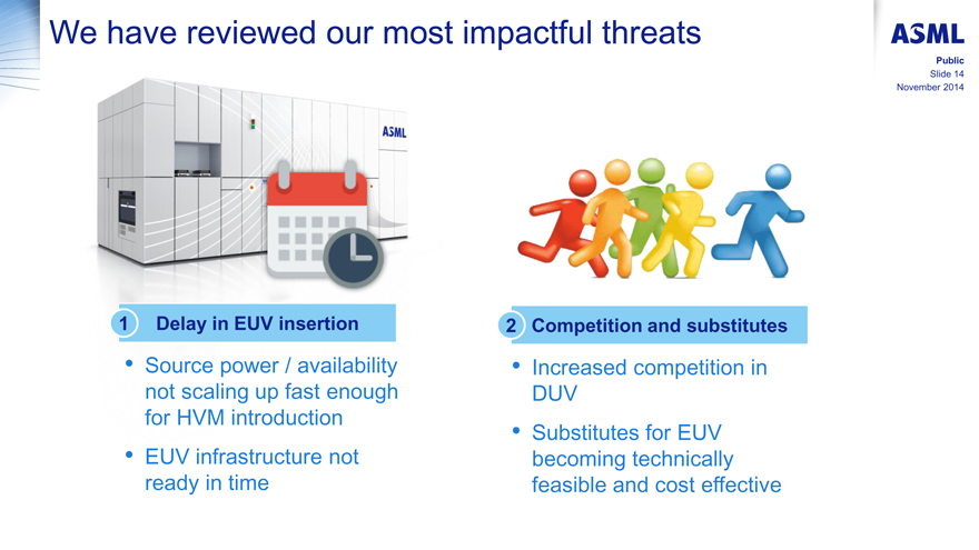
We have reviewed our most impactful threats
ASML Public Slide 14 November 2014
ASML
1 Delay in EUV insertion
Source power / availability not scaling up fast enough for HVM introduction
EUV infrastructure not ready in time
2 Competition and substitutes
Increased competition in DUV
Substitutes for EUV becoming technically feasible and cost effective
�
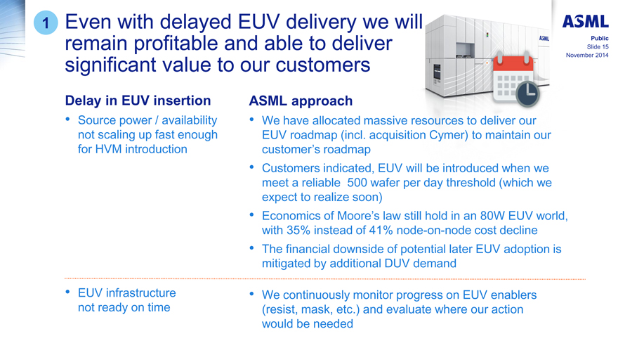
1 Even with delayed EUV delivery we will remain profitable and able to deliver significant value to our customers
ASML ASML Public Slide 15 November 2014
Delay in EUV insertion
Source power / availability not scaling up fast enough for HVM introduction
EUV infrastructure not ready on time
ASML approach
We have allocated massive resources to deliver our EUV roadmap (incl. acquisition Cymer) to maintain our customer�s roadmap
Customers indicated, EUV will be introduced when we meet a reliable 500 wafer per day threshold (which we expect to realize soon)
Economics of Moore�s law still hold in an 80W EUV world, with 35% instead of 41% node-on-node cost decline
The financial downside of potential later EUV adoption is mitigated by additional DUV demand
We continuously monitor progress on EUV enablers (resist, mask, etc.) and evaluate where our action would be needed
�
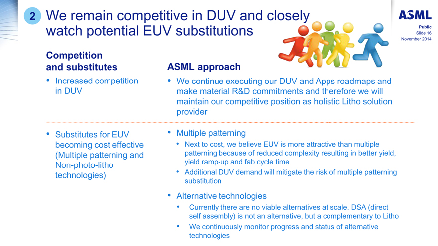
2 We remain competitive in DUV and watch potential EUV substitutions
ASML Public Slide 16 November 2014
Competition and substitutes
Increased competition in DUV
Substitutes for EUV becoming cost effective (Multiple patterning and Non-photo-litho technologies)
ASML approach
We continue executing our DUV and Apps roadmaps and make material R&D commitments and therefore we will maintain our competitive position as holistic Litho solution provider
Multiple patterning
Next to cost, we believe EUV is more attractive than multiple patterning because of reduced complexity resulting in better yield, yield ramp-up and fab cycle time
Additional DUV demand will mitigate the risk of multiple patterning substitution
Alternative technologies
Currently there are no viable alternatives at scale. DSA (direct self assembly) is not an alternative, but a complementary to Litho
We continuously monitor progress and status of alternative technologies
�
Summary: ASML�s positioning, opportunities and threats
ASML Public Slide 17 November 2014
ASML�s prime responsibility is to provide value for our customers, shareholders, employees, and supply chain partners
Our success is based on delivering Litho products with superior performance at lowest cost of ownership and on our flexible operating model required for an inherently volatile market
ASML models an annual total revenue opportunity of 10B€ by 2020 and subsequent growth beyond
We have reviewed our most impactful threats and feel confident about our approach to mitigate these

�
ASML
INVESTOR DAY
ASMLSMALLTALK2014
LONDON
Exhibit 99.3
�
�
ASML
Many ways to shrink:
The right moves to 10 nanometer and beyond
Martin van den Brink
President�& Chief Technology Officer
24�November 2014
INVESTOR DAY
ASMLSMALLTALK2014
LONDON
�
Forward looking statements
ASML
Public
Slide 2
November 2014
This document contains statements relating to certain projections and business trends that are forward-looking, including statements with respect to our outlook, expected customer demand in specified market segments, expected sales levels and trends, our market share, customer orders and systems backlog, IC unit demand, expected or indicative financial results or targets, including revenue, gross margin, expenses, gross margin percentage, opex percentage of sales, tax percentage, cash conversion cycle, capex percentage of sales, credit rating and earnings per share, expected shipments of tools and the timing thereof, including expected shipments of EUV and DUV tools, productivity of our tools and systems performance, including EUV system performance (such as endurance tests), the development of EUV technology and timing of shipments, development in IC technology, including shrink scenarios, NAND technology development and cost estimates, expectations on development of the shrink roadmap across all of our systems, upgradeability of our tools, system orders, customer transition estimates, expected transition scaling, forecasted industry developments, including expected smartphone, tablet and server use in future years, and expectations relating to new applications including wearable devices and connected devices, expected investment pay-back time for foundries, expected construction of additional holistic lithography infrastructure, the continuation of Moore�s Law, and our dividend policy and intention to repurchase shares. You can generally identify these statements by the use of words like �may�, �will�, �could�, �should�, �project�, �believe�, �anticipate�, �expect�, �plan�, �estimate�, �forecast�, �potential�, �intend�, �continue� and variations of these words or comparable words. These statements are not historical facts, but rather are based on current expectations, estimates, assumptions and projections about the business and our future financial results and readers should not place undue reliance on them.
Forward-looking statements do not guarantee future performance and involve risks and uncertainties. These risks and uncertainties include, without limitation, economic conditions, product demand and semiconductor equipment industry capacity, worldwide demand and manufacturing capacity utilization for semiconductors (the principal product of our customer base), the impact of general economic conditions on consumer confidence and demand for our customers� products, competitive products and pricing, affordability of shrink, the continuation of Moore�s Law, the impact of manufacturing efficiencies and capacity constraints, performance of our systems, the continuing success of technology advances and the related pace of new product development and customer acceptance of new products and customers meeting their own development roadmaps, market demand for our existing products and for new products and our ability to maintain or increase or market share, the development of and customer demand for multi-patterning technology and our ability to meet overlay and patterning requirements, the number and timing of EUV systems expected to be shipped, our ability to enforce patents and protect intellectual property rights, the risk of intellectual property litigation, EUV system performance and customer acceptance, availability of raw materials and critical manufacturing equipment, trade environment, our ability to reduce costs, changes in exchange rates and tax rates, available cash, distributable reserves for dividend payments and share repurchases, changes in our treasury policy, including our dividend and repurchase policy, completion of sales orders, the risk that key assumptions underlying financial targets prove inaccurate, including assumptions relating to market share, lithography market growth and our customers� ability to reduce productions costs, risks associated with Cymer, which we acquired in 2013, and other risks indicated in the risk factors included in ASML�s Annual Report on Form 20-F and other filings with the US Securities and Exchange Commission. These forward-looking statements are made only as of the date of this document. We do not undertake to update or revise the forward-looking statements, whether as a result of new information, future events or otherwise.
�
ASML
Public
Slide 3
November 2014
Content
Industry Challenges
The desire to shrink
The device challenges
The scaling challenges
ASML Solutions
Our holistic approach to extend immersion
The process simplification by using EUV
�
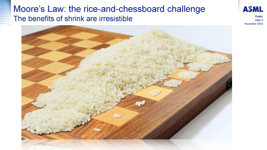
Moore�s Law: the rice-and-chessboard challenge
The benefits of shrink are irresistible
ASML
Public
Slide 4
November 2014
�
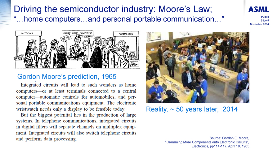
Driving the semiconductor industry: Moore�s Law;
�...home computers... and personal portable communication...�
ASML
Public
Slide 5
November 2014
Gordon Moore�s prediction, 1965
Integrated circuits will lead to such wonders as home computers�or at least terminals connected to a central computer�automatic controls for automobiles, and personal portable communications equipment. The electronic wristwatch needs only a display to be feasible today.
But the biggest potential lies in the production of large systems. In telephone communications, integrated circuits in digital filters will separate channels on multiplex equipment. Integrated circuits will also switch telephone circuits and perform data processing.
Reality, ~ 50 years later, 2014
Source: Gordon E. Moore,
�Cramming More Components onto Electronic Circuits�,
Electronics, pp114-117,�April�19, 1965
�
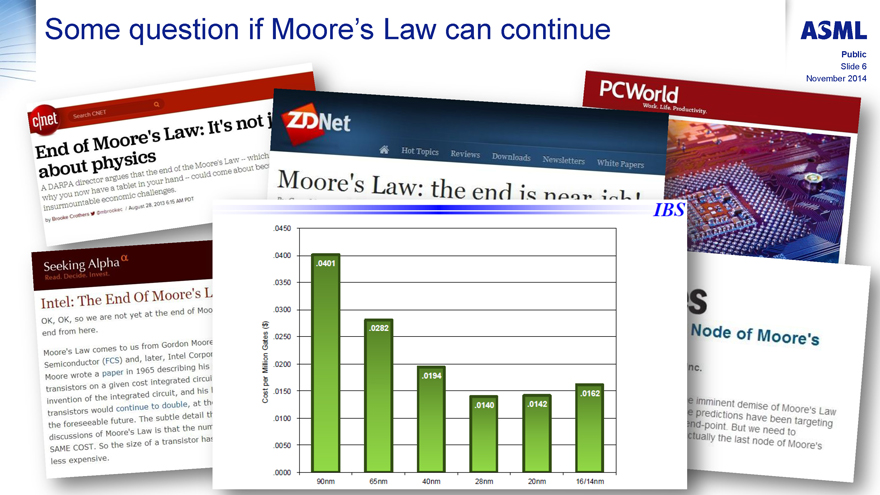
Some question if Moore�s Law can continue
ASML
Public
Slide 6
November 2014
C|net Search CNET
End of Moore�s Law: It�s not
about physics
A DARPA director argues that the end of the Moore�s law � which why you now have a tablet in your hand � could come about bec insurmountable economic challenges
by Brooke Crothers @mbrookec August�28, 2013 6:15 AM PDT
ZDNet
Hot Topics
Reviews
Downloads
Newsletters
White Papers
Moore�s Law: the end is near
PCWorld
Work, Life productivity
Seeking Alpha
Read. Decide. Invest.
Intel: The End of Moore�s
OK, OK, so we are not yet at the end of Moo
end from here.
Moore�s law comes to us from Gordon Moore
Semiconductor (FCS) and, later, Intel Corpo
Moore wrote a paper in 1965 describing his transistors on a given cost integrated circuit invention of the integrated circuit, and his transistor would continue to double, at the foreseeable future. The subtle detail discussions of Moore�s law is that the SAME COST. So the size of a transistor has less expensive.
Cost per Million Gates ($)
.0450
.0400
.0350
.0300
.0250
.0200
.0150
.0100
.0050
.0000
.0401
90nm
.0282
65nm
.0194
40nm
.0140
28nm
.0142
20nm
.0162
16/14nm
�
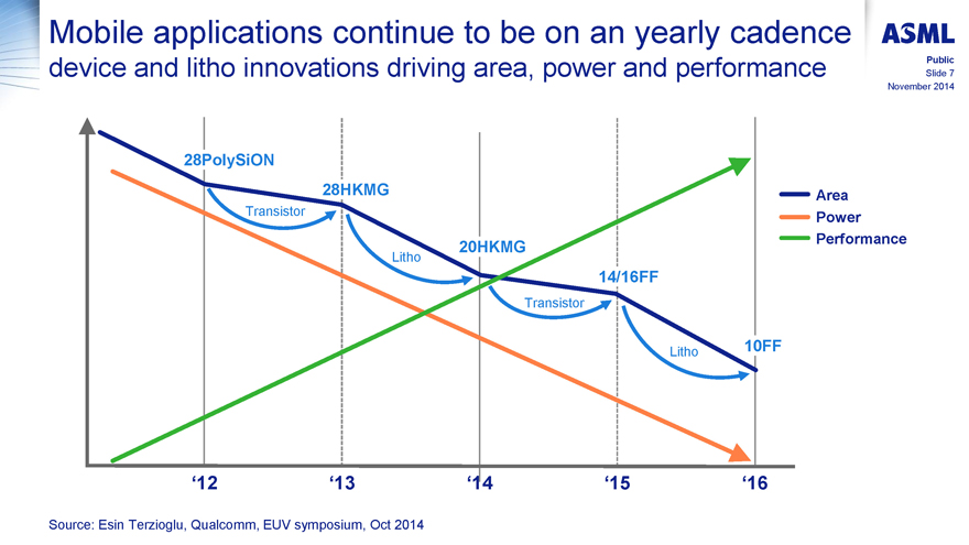
Mobile applications continue to be on an yearly cadence device and litho innovations driving area, power and performance
ASML
Public
Slide 7
November 2014
28PolySiON
28HKMG Area
Transistor Power
20HKMG Performance
Litho
14/16FF
Transistor
Litho 10FF
�12 �13 �14 �15 �16
Source: Esin Terzioglu, Qualcomm, EUV symposium, Oct 2014
�
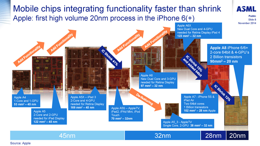
Mobile chips integrating functionality faster than shrink
Apple: first high volume 20nm process in the iPhone 6(+)
ASML
Public
Slide 8
November 2014
Add Functionality
Add Functionality
IC Shrink 41%
Add Functionality
Add Functionality
Apple A6x
New Dual Core and 4-GPU needed for Retina Display iPad 4 123 mm2 - 32 nm
IC Shrink 15% and added 64bit
Apple A4 1-Core and 1-GPU 53 mm2 - 45 nm
Apple A5 2-Core and 2GPU needed for iPad Display 122 mm2 � 45 nm
Apple A5X - iPad 3 2-Core and 4-GPU needed for Retina Display 169 mm2 - 45 nm
Apple A5S � Apple TV, iPad2, iPad Mini, ipod Touch 70 mm2 - 32nm
De-featuring
Apple A5_3 - Apple TV Single Core, 2-GPU 38 mm2 - 32 nm
Apple A7 - iPhone 5S�& iPad Air Two 64bit cores 1 Billion transistors 102 mm2 - 28 nm Apple
IC Shrink 12%
45nm
32nm
28nm
20nm
Source: Apple
�
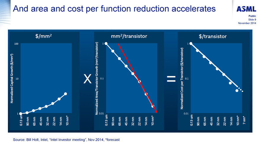
And area and cost per function reduction accelerates
ASML
Public
Slide 9�November 2014
$/mm2
Normalized Capital Growth ($/mm2)
100
10
1
0.13 um
90 nm
65 nm
45 nm
32 nm
22 nm
14 nm
10 nm*
X
mm2/transistor
Normalized Area/Transistor Growth (mm2/transistor)
1
0.1
0.01
0.13 um
90 nm
65 nm
45 nm
32 nm
22 nm
14 nm
10 nm*
=
$/transistor
Normalized Cost per Transistor ($/transistor)
1
0.1
0.01
0.13 um
90 nm
65 nm
45 nm
32 nm
22 nm
14 nm
10 nm*
7 nm*
Source: Bill Holt, Intel, �Intel Investor meeting�, Nov 2014, *forecast
�
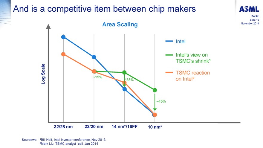
And is a competitive item between chip makers
ASML
Public
Slide 10
November 2014
Area Scaling
Log Scale
~15%
*35%
~45%
Intel
Intel�s view on TSMC�s shrink1
TSMC reaction on Intel2
32/28 nm 22/20 nm 14 nm*/16FF 10 nm*
Sourcews:
1Bill Holt, Intel investor conference, Nov 2013
2Mark Liu, TSMC analyst call, Jan 2014
�
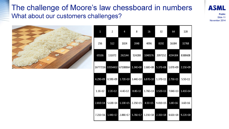
The challenge of Moore�s law chessboard in numbers
What about our customers challenges?
ASML
Public
Slide 11
November 2014
1 2 4 8 16 32 64 128
256 512 1024 2048 4096 8192 16384 32768
65536 131072 262144 524288 1048576 2097152 4194304 8388608
16777216 33554432 67108864 1.34E+08 5.37E+08 1.07E+09 2.15E+09
4.29E+09 8.59E+09 1.72E+10 3.44E+10 6.87E+10 1.37E+11 2.75E+11 5.5E+11
1.1E+12 2.2E+12 4.4E+12 8.8E+12 1.76E+13 3.52E+13 7.04E+13 1.41E+14
2.81E+14 5.63E+14 1.13E+15 2.2E+15 4.5E+15 9.01E+15 1.8E+16 3.6E+16
7.21E+16 1.44E+17 2.88E+17 5.76E+17 1.15E+18 2.31E+18 4.61E+18 9.22E+18
�
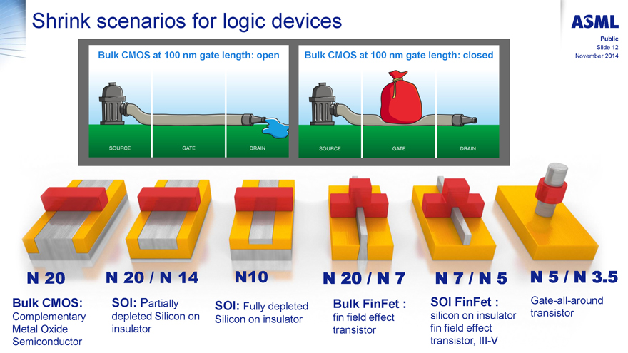
Shrink scenarios for logic devices
ASML
Public
Slide 12
November 2014
Bulk CMOS at 100 nm gate length: open
SOURCE GATE DRAIN
Bulk CMOS at 100 nm gate length: closed
SOURCE GATE DRAIN
N 20
Bulk CMOS:
Complementary Metal Oxide Semiconductor
N 20 / N 14
SOI: Partially depleted Silicon on insulator
N10
SOI: Fully depleted Silicon on insulator
N 20 / N 7
Bulk FinFet :
fin field effect transistor
N 7 / N 5
SOI FinFet :
silicon on insulator fin field effect transistor, III-V
N 5 / N 3.5
Gate-all-around transistor
�
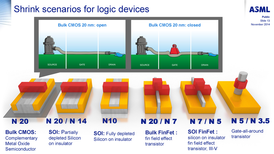
Shrink scenarios for logic devices
ASML
Public
Slide 13
November 2014
Bulk CMOS 20 nm: open
SOURCE GATE DRAIN
Bulk CMOS 20 nm: closed
SOURCE GATE DRAIN
N 20
Bulk CMOS:
Complementary Metal Oxide Semiconductor
N 20 / N 14
SOI: Partially depleted Silicon on insulator
N10
SOI: Fully depleted Silicon on insulator
N 20 / N 7
Bulk FinFet :
fin field effect transistor
N 7 / N 5
SOI FinFet :
silicon on insulator fin field effect transistor, III-V
N 5 / N 3.5
Gate-all-around transistor
�
Shrink scenarios for logic devices
ASML
Public
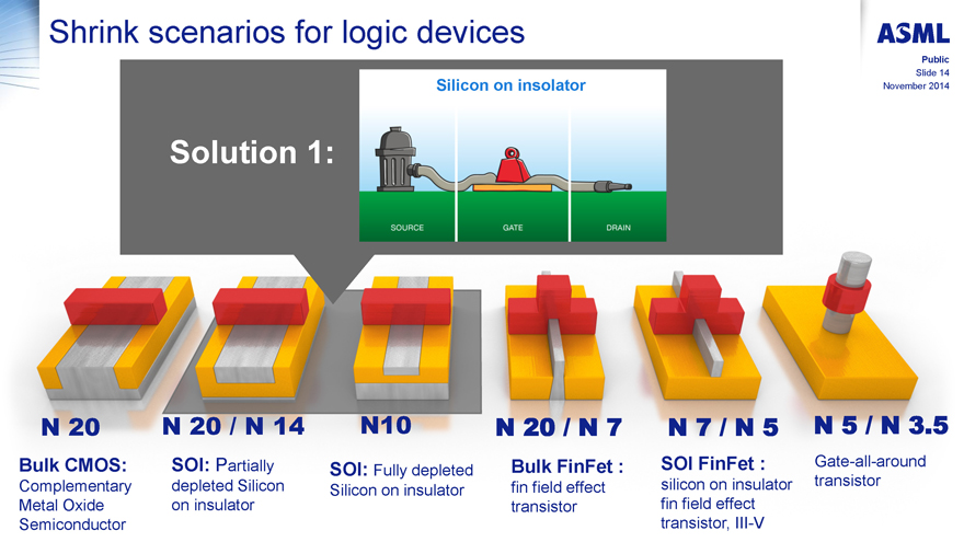
Slide 14
November 2014
Solution 1:
Silicon on insolator
SOURCE GATE DRAIN
N 20
Bulk CMOS:
Complementary Metal Oxide Semiconductor
N 20 / N 14
SOI: Partially depleted Silicon on insulator
N10
SOI: Fully depleted Silicon on insulator
N 20 / N 7
Bulk FinFet :
fin field effect transistor
N 7 / N 5
SOI FinFet :
silicon on insulator fin field effect transistor, III-V
N 5 / N 3.5
Gate-all-around transistor
�
Shrink scenarios for logic devices
ASML
Public
Slide 15
November 2014
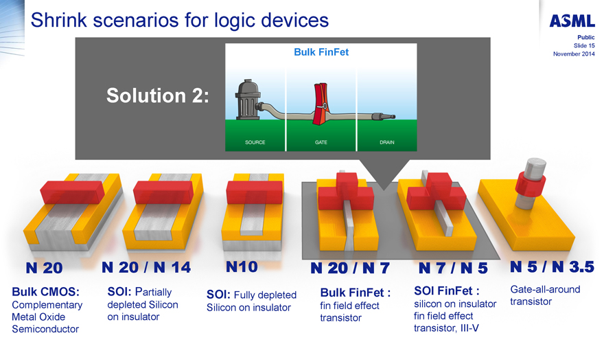
Solution 2:
Bulk FinFet
SOURCE GATE DRAIN
N 20
Bulk CMOS:
Complementary Metal Oxide Semiconductor
N 20 / N 14
SOI: Partially depleted Silicon on insulator
N10
SOI: Fully depleted Silicon on insulator
N 20 / N 7
Bulk FinFet :
fin field effect transistor
N 7 / N 5
SOI FinFet :
silicon on insulator fin field effect transistor, III-V
N 5 / N 3.5
Gate-all-around transistor
�
Shrink scenarios for logic devices
ASML
Public
Slide 16
November 2014
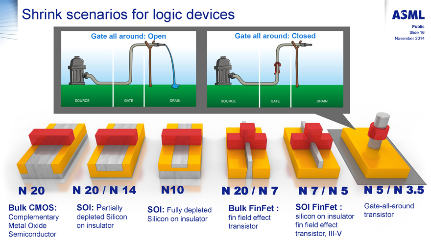
Gate all around: Open
SOURCE GATE DRAIN
Gate all around: Closed
SOURCE GATE DRAIN
N 20
Bulk CMOS:
Complementary Metal Oxide Semiconductor
N 20 / N 14
SOI: Partially depleted Silicon on insulator
N10
SOI: Fully depleted Silicon on insulator
N 20 / N 7
Bulk FinFet :
fin field effect transistor
N 7 / N 5
SOI FinFet :
silicon on insulator fin field effect transistor, III-V
N 5 / N 3.5
Gate-all-around transistor
�
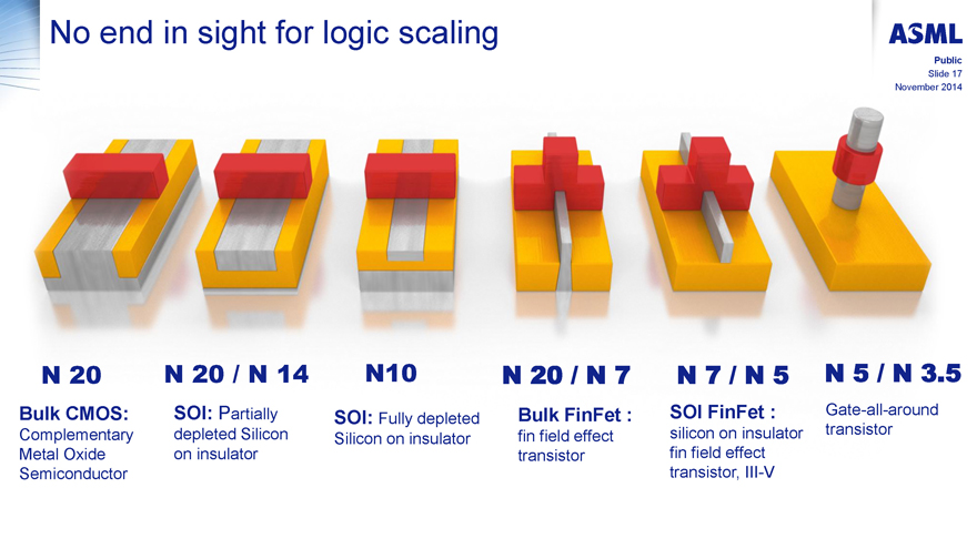
No end in sight for logic scaling
ASML
Public
Slide 17
November 2014
N 20
Bulk CMOS:
Complementary Metal Oxide Semiconductor
N 20 / N 14
SOI: Partially depleted Silicon on insulator
N10
SOI: Fully depleted Silicon on insulator
N 20 / N 7
Bulk FinFet :
fin field effect transistor
N 7 / N 5
SOI FinFet :
silicon on insulator fin field effect transistor, III-V
N 5 / N 3.5
Gate-all-around transistor
�
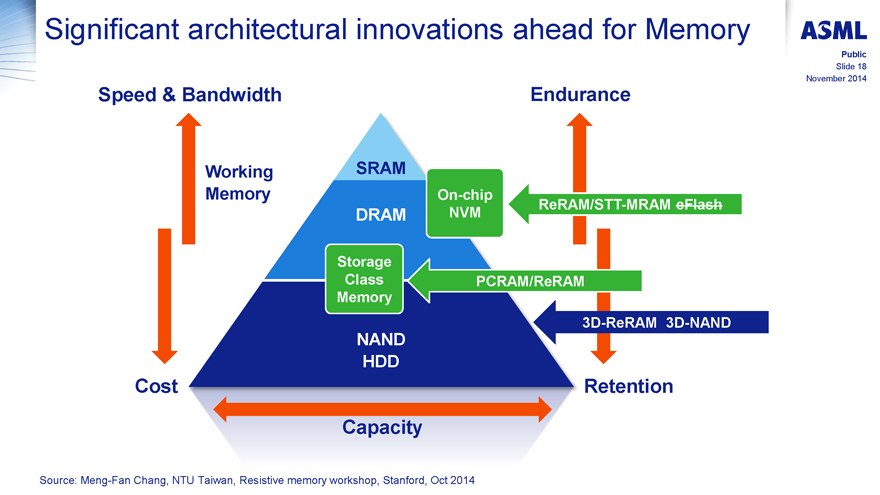
Significant architectural innovations ahead for Memory
ASML
Public
Slide 18
November 2014
Speed & Bandwidth
Working Memory
Cost
SRAM
DRAM
Storage Class Memory
NAND HDD
On-chip NVM
Endurance
ReRAM/STT-MRAM eFlash
PCRAM/ReRAM
3D-ReRAM 3D-NAND
Retention
Capacity
Source: Meng-Fan Chang, NTU Taiwan, Resistive memory workshop, Stanford, Oct 2014
�
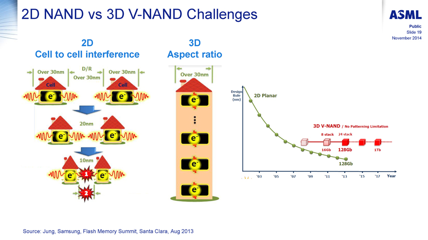
2D NAND vs 3D V-NAND Challenges
ASML
Public
Slide 19
November 2014
2D Cell to cell interference
Over 30nm D/R Over 30nm Over 30nm
Cell Cell
e- e-
20nm
e- e-
10nm
e- e-
1 2
3D Aspect ratio
Over 30nm
e-
e-
e-
e-
Design Rule (nm)
2D Planar
3D V-NAND / No Patterning Limitation
8 stack 24 stack
16Gb 128Gb 1Tb
128Gb
�03 �05 �07 �09 �11 �13 �15 �17 Year
Source: Jung, Samsung, Flash Memory Summit, Santa Clara, Aug 2013
�
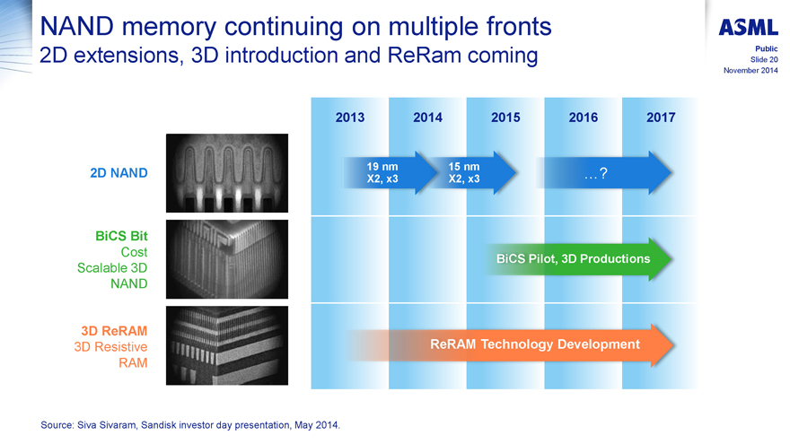
NAND memory continuing on multiple fronts
2D extensions, 3D introduction and ReRam coming
ASML
Public
Slide 20
November 2014
2D NAND
BiCS Bit
Cost
Scalable 3D
NAND
3D ReRAM
3D Resistive
RAM
2013 2014 2015 2016 2017
19 nm 15 nm �? X2, x3 X2, x3
BiCS Pilot, 3D Productions
ReRAM Technology Development
Source: Siva Sivaram, Sandisk investor day presentation, May 2014.
�
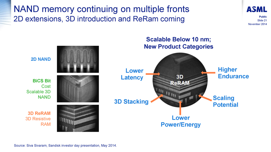
NAND memory continuing on multiple fronts
2D extensions, 3D introduction and ReRam coming
ASML
Public
Slide 21
November 2014
2D NAND
BiCS Bit
Cost
Scalable 3D
NAND
3D ReRAM
3D Resistive
RAM
Scalable Below 10 nm; New Product Categories
Lower Latency
3D Stacking
Lower Power/Energy
Scaling Potential
Higher Endurance
3D ReRAM
Source: Siva Sivaram, Sandisk investor day presentation, May 2014.
�
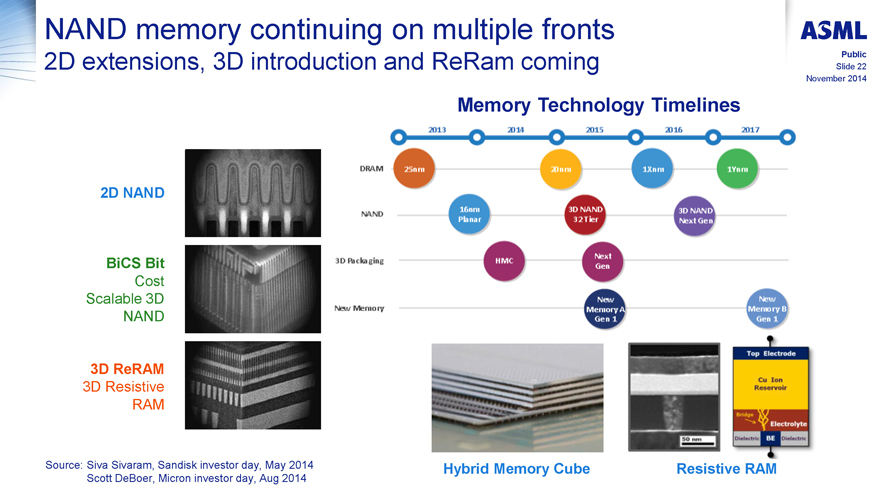
NAND memory continuing on multiple fronts
2D extensions, 3D introduction and ReRam coming
ASML
Public
Slide 22
November 2014
2D NAND
BiCS Bit
Cost
Scalable 3D
NAND
3D ReRAM
3D Resistive
RAM
Memory Technology Timelines
2013 2014 2015 2016 2017
DRAM 25nm 20nm 1Xnm 1Ynm
NAND 16nm Planar 3D NAND 32Tier 3D NAND Next Gen
3D Packaging HMC Next Gen
New Memory New Memory A Gen 1 New Memory B Gen 1
50 nm
Top Electrode
Cu Ion Reservoir
Bridge
Electrolyte
Dielectric BE Dielectric
Hybrid Memory Cube
Resistive RAM
Source: Siva Sivaram, Sandisk investor day, May 2014
Scott DeBoer, Micron investor day, Aug 2014
�
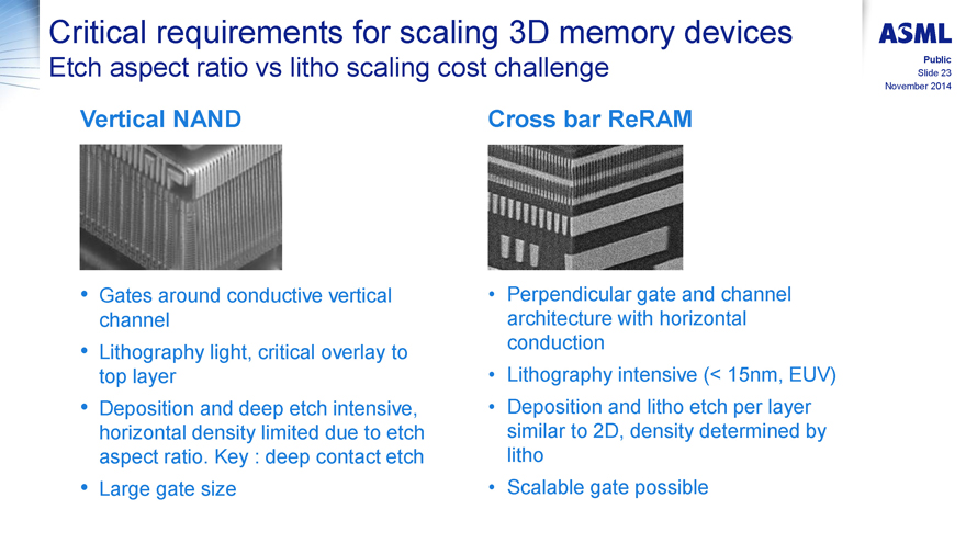
Critical requirements for scaling 3D memory devices
Etch aspect ratio vs litho scaling cost challenge
ASML
Public
Slide 23
November 2014
Vertical NAND
Gates around conductive vertical channel
Lithography light, critical overlay to top layer
Deposition and deep etch intensive, horizontal density limited due to etch aspect ratio. Key : deep contact etch
Large gate size
Cross bar ReRAM
Perpendicular gate and channel architecture with horizontal conduction
Lithography intensive (< 15nm, EUV)
Deposition and litho etch per layer similar to 2D, density determined by litho
Scalable gate possible
�
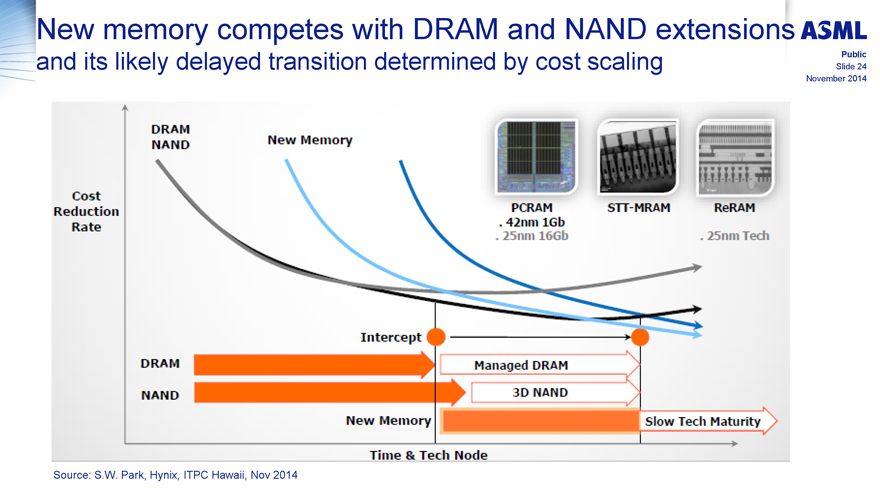
New memory competes with DRAM and NAND extensions
and its likely delayed transition determined by cost scaling
ASML
Public
Slide 24
November 2014
Cost Reduction Rate
DRAM NAND
New Memory
PCRAM . 42nm 1Gb . 25nm 16Gb
STT-MRAM
ReRAM . 25nm Tech
Intercept
DRAM Managed DRAM
NAND 3D NAND
New Memory Slow Tech Maturity
Time�& Tech Node
Source: S.W. Park, Hynix, ITPC Hawaii, Nov 2014
�
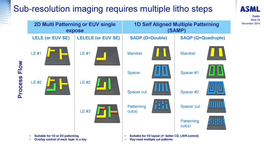
Sub-resolution imaging requires multiple litho steps
ASML
Public
Slide 25
November 2014
Process Flow
2D Multi Patterning or EUV single expose
LELE (or EUV SE)
LE #1 LE #2
LELELE (or EUV SE)
LE #1 LE #2 LE #3
1D Self Aligned Multiple Patterning (SAMP)
SADP (D=Double)
Mandrel
Spacer
Spacer cut
Patterning cut(s)
SAQP (Q=Quadruple)
Mandrel
Spacer #1
Spacer #2
Spacer cut
Patterning cut(s)
Suitable for 1D or 2D patterning
Overlay control of each layer is a key
Suitable for 1D layout ( better CD, LWR control)
May need multiple cut patterns
�
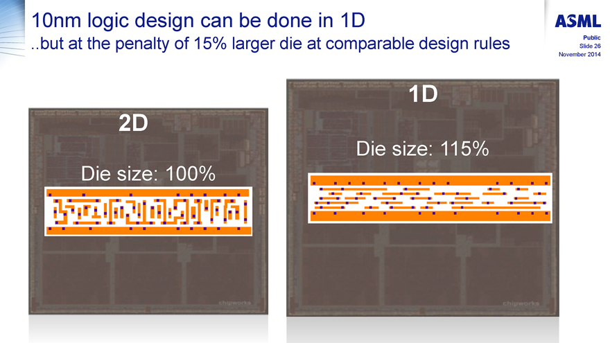
10nm logic design can be done in 1D
..but at the penalty of 15% larger die at comparable design rules
2D
Die size: 100%
1D
Die size: 115%
ASML
Public
Slide 26
November 2014
�
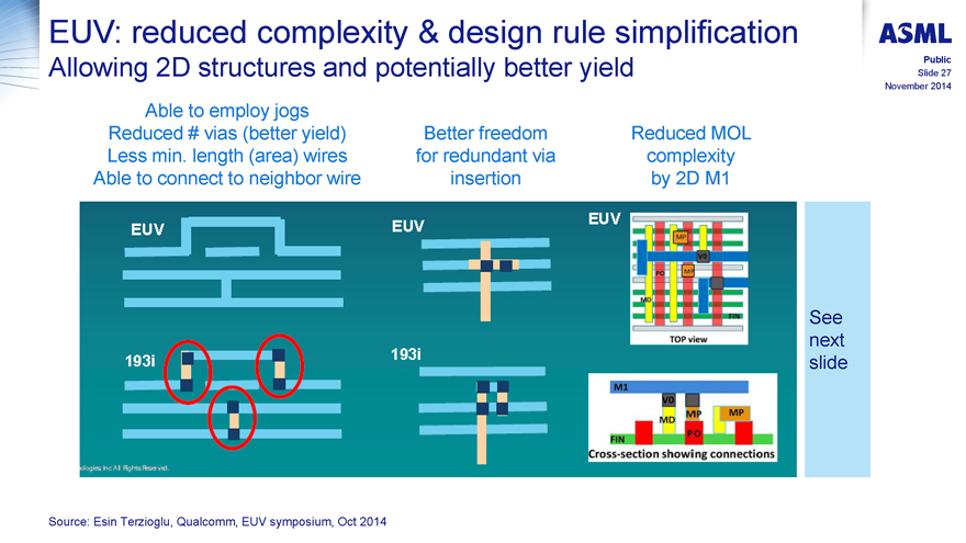
EUV: reduced complexity�& design rule simplification
Allowing 2D structures and potentially better yield
ASML
Public
Slide 27
November 2014
Able to employ jogs Reduced # vias (better yield) Less min. length (area) wires Able to connect to neighbor wire
Better freedom for redundant via insertion
Reduced MOL complexity by 2D M1
EUV
193i
EUV
193i
EUV
MP
V0
PO
MP
MD
TIN
TOP view
M1
V0
MD
MP
MP
FIN
PO
Cross-section showing connections
See next slide
Source: Esin Terzioglu, Qualcomm, EUV symposium, Oct 2014
�
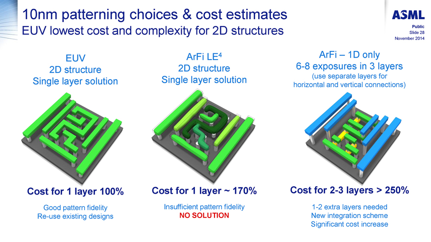
10nm patterning choices�& cost estimates
EUV lowest cost and complexity for 2D structures
ASML
Public
Slide 28
November 2014
EUV 2D structure Single layer solution
Cost for 1 layer 100%
Good pattern fidelity Re-use existing designs
ArFi LE4 2D structure Single layer solution
Cost for 1 layer ~ 170%
Insufficient pattern fidelity
NO SOLUTION
ArFi � 1D only 6-8 exposures in 3 layers (use separate layers for horizontal and vertical connections)
Cost for 2-3 layers > 250%
1-2 extra layers needed New integration scheme Significant cost increase
�
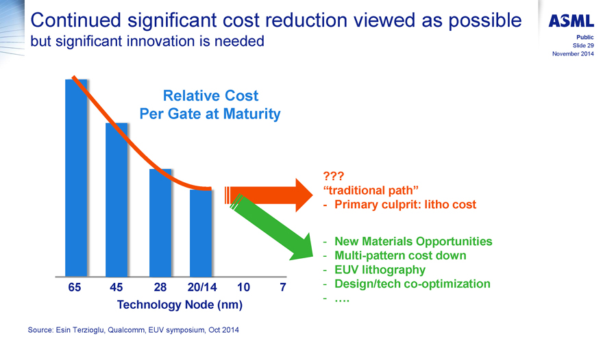
Continued significant cost reduction viewed as possible
but significant innovation is needed
ASML
Public
Slide 29
November 2014
Relative Cost Per Gate at Maturity
65 45 28 20/14 107
Technology Node (nm)
???
�traditional path�
- Primary culprit: litho cost
- New Materials Opportunities
- Multi-pattern cost down
- EUV lithography
- Design/tech co-optimization
- �.
Source: Esin Terzioglu, Qualcomm, EUV symposium, Oct 2014
�
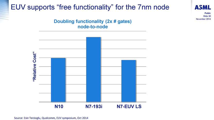
EUV supports �free functionality� for the 7nm node
ASML
Public
Slide 30
November 2014
Doubling functionality (2x # gates) node-to-node
�Relative Cost�
N10 N7-193i N7-EUV LS
Source: Esin Terzioglu, Qualcomm, EUV symposium, Oct 2014
�
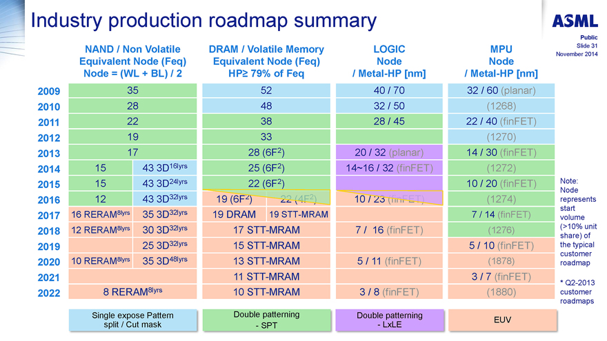
Industry production roadmap summary
ASML
Public
Slide 31
November 2014
NAND / Non Volatile Equivalent Node (Feq) Node = (WL + BL) / 2
DRAM / Volatile Memory Equivalent Node (Feq) HP� 79% of Feq
LOGIC Node / Metal-HP [nm]
MPU Node / Metal-HP [nm]
2009 35 52 40 / 70 32 / 60 (planar)
2010 28 48 32 / 50 (1268)
2011 22 38 28 / 45 22 / 40 (finFET)
2012 19 33 (1270)
2013 17 28 (6F2) 20 / 32 (planar) 14 / 30 (finFET)
2014 15 43 3D16lyrs 25 (6F2) 14~16 / 32 (finFET) (1272)
2015 15 43 3D24lyrs 22 (6F2) 10 / 20 (finFET)
2016 12 43 3D32lyrs 19 (6F2) 22 (4F2) 10 / 23 (finFET) (1274)
2017 16 RERAM8lyrs 35 3D32lyrs 19 DRAM 19 STT-MRAM 7 / 14 (finFET)
2018 12 RERAM8lyrs 30 3D32lyrs 17 STT-MRAM 7 / 16 (finFET) (1276)
2019 25 3D32lyrs 15 STT-MRAM 5 / 10 (finFET)
2020 10 RERAM8lyrs 35 3D48lyrs 13 STT-MRAM 5 / 11 (finFET) (1878)
2021 11 STT-MRAM 3 / 7 (finFET)
2022 8RERAM8lyrs 10 STT-MRAM 3 / 8 (finFET) (1880)
Single expose Pattern split / Cut mask
Double patterning - SPT
Double patterning - LxLE
EUV
Note: Node represents start volume (>10% unit share) of the typical customer roadmap
* Q2-2013 customer roadmaps
�
Industry production roadmap summary
ASML
Public
Slide 32
November 2014
NAND / Non Volatile Equivalent Node (Feq) Node = (WL + BL) / 2
DRAM / Volatile Memory Equivalent Node (Feq) HP� 79% of Feq
LOGIC Node / Metal-HP [nm]
MPU Node / Metal-HP [nm]
2009 35 52 40 / 70 32 / 60 (planar)
2010 28 48 32 / 50 (1268)
2011 22 38 22 / 40 (finFET)
2012 19 (1270)
2013 17 14 / 30 (finFET)
2014 16lyrs
2015 24lyrs
2016 32lyrs 19 (6F2) 22 (4F2) 10 / 23 (finFET)
2017 16 RERAM8lyrs 35 3D32lyrs 19 DRAM 19 STT-MRAM
2018 12 RERAM8lyrs 30 3D32lyrs 17 STT-MRAM 7 / 16 (finFET) (1276)
2019 25 3D32lyrs 15 STT-MRAM 5 / 10(finFET)
2020 10 RERAM8lyrs 35 3D48lyrs 13 STT-MRAM 5 / 11 (finFET) (1878)
2021 11 STT-MRAM 3 / 7 (finFET)
2022 8RERAM8lyrs 10 STT-MRAM 3 / 8 (finFET) (1880)
Single expose Pattern split / Cut mask
Double patterning - SPT
Double patterning - LxLE
EUV
Note: Node represents start volume (>10% unit share) of the typical customer roadmap
* Q2-2013 customer roadmaps
Estimated NAND EUV insertion
Estimated DRAM EUV insertion
Estimated Logic EUV insertion
Estimated MPU EUV insertion
�
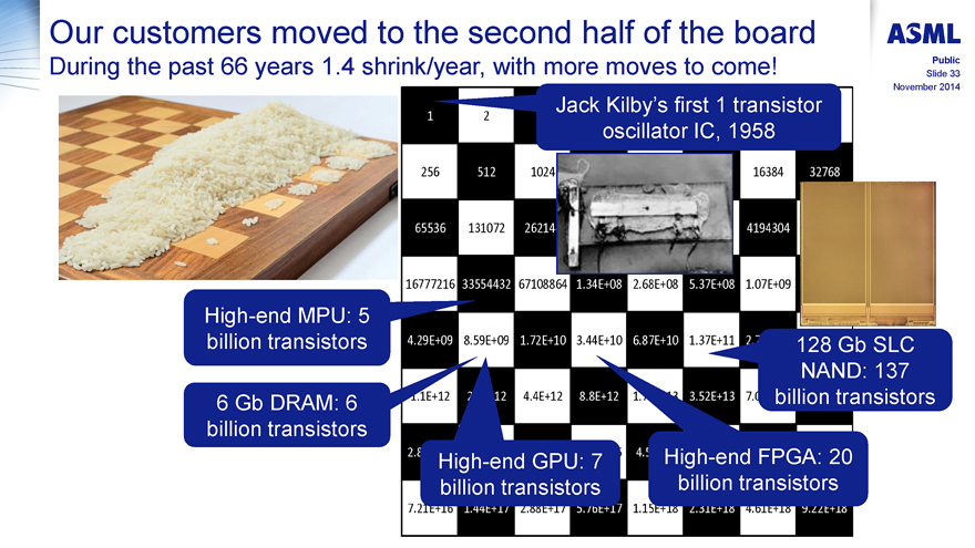
Our customers moved to the second half of the board
During the past 66 years 1.4 shrink/year, with more moves to come!
ASML
Public
Slide 33
November 2014
High-end MPU: 5 billion transistors
6 Gb DRAM: 6 billion transistors
Jack Kilby�s first 1 transistor oscillator IC, 1958
High-end GPU: 7 billion transistors
High-end FPGA: 20 billion transistors
128 Gb SLC NAND: 137 billion transistors
12
256 512 1024 16384 32768
65536 131072 26214 4194304
16777216 33554432 67108864 1.34E+08 2.68E+08 5.37E+08 1.07E+09
4.29E+09 8.59E+09 1.72E+10 3.44E+10 6.87E+10 1.37E+11 2.7
1.1E+12 12 4.4E+12 8.8E+12 1 3.52E+13 7.0
2.8 4.5
7.21E+16 1.44E+17 2.88E+17 5.76E+17 1.15E+18 2.31E+18 4.61E+18 9.22E+18
�
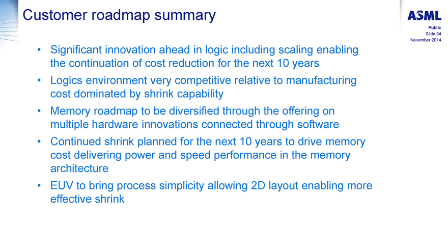
Customer roadmap summary
ASML
Public
Slide 34
November 2014
Significant innovation ahead in logic including scaling enabling the continuation of cost reduction for the next 10 years
Logics environment very competitive relative to manufacturing cost dominated by shrink capability
Memory roadmap to be diversified through the offering on multiple hardware innovations connected through software
Continued shrink planned for the next 10 years to drive memory cost delivering power and speed performance in the memory architecture
EUV to bring process simplicity allowing 2D layout enabling more effective shrink
�
ASML
Public
Slide 35
November 2014
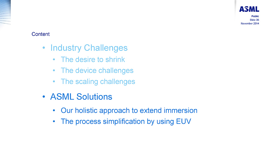
Content
Industry Challenges
The desire to shrink
The device challenges
The scaling challenges
ASML Solutions
Our holistic approach to extend immersion
The process simplification by using EUV
�
ASML
Public
Slide 36
November 2014
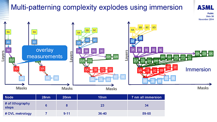
Multi-patterning complexity explodes using immersion
5A 5A 5A 5B 5C 5A 5B 5C 5D
4A 4A 4A 4B 4C 4A 4B
3A overlay measurements 3A 3B 3C 3D 3A 3B 3C 3D 3E
Layers 21A Layers 21A 21B 22A 22B
Layers 21A 21B 21C 21D 21E 21F 21G 21H 21I 22A 22B 22C
1A 1A 1A 1B 1C 1D 1A 1B 1C 1D 1E 1F Immersion
0A 0A 0B 0A 0B 0C 0D 0E 0A 0B 0C 0D 0E
Masks Masks Masks Masks
Node 28nm 20nm 10nm 7 nm all immersion
# of lithography steps 6 8 23 34
# OVL metrology 7 9-11 36-40 59-65
�
ASML
Public
Slide 37
November 2014
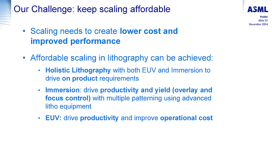
Our Challenge: keep scaling affordable
Scaling needs to create lower cost and improved performance
Affordable scaling in lithography can be achieved:
Holistic Lithography with both EUV and Immersion to drive on product requirements
Immersion: drive productivity and yield (overlay and focus control) with multiple patterning using advanced litho equipment
EUV: drive productivity and improve operational cost
�
ASML
Public
Slide 38
November 2014
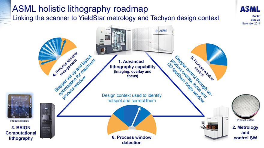
ASML holistic lithography roadmap
Linking the scanner to YieldStar metrology and Tachyon design context
4. Process window enlargement
Stepper set up and layout optimization for maximum process window
1. Advanced lithography capability (Imaging, overlay and focus)
5. Process window control
Stepper control through on-product overlay, focus and CD feedback loops window
Product reticles
Design context used to identify hotspot and correct them
Product wafers
3. BRION Computational lithography
6. Process window detection
2. Metrology and control SW
�
ASML
Public
Slide 39
November 2014
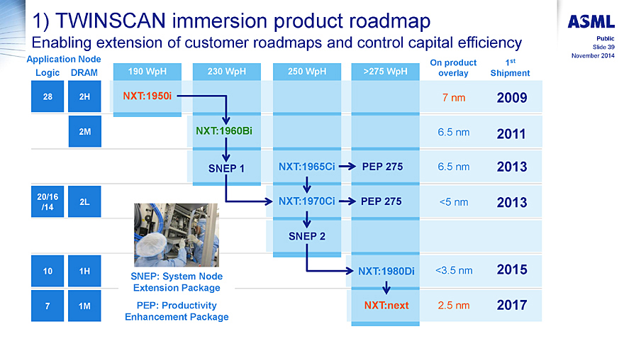
1) TWINSCAN immersion product roadmap
Enabling extension of customer roadmaps and control capital efficiency
Application Node On product 1st
Logic DRAM 190 WpH 230 WpH 250 WpH >275 WpH overlay Shipment
28 2H NXT:1950i 7 nm 2009
2M NXT:1960Bi 6.5 nm 2011
SNEP 1 NXT:1965Ci PEP 275 6.5 nm 2013
20/16/14 2L NXT:1970Ci PEP 275 <5 nm 2013
SNEP 2
10 1H NXT:1980Di <3.5 nm 2015
SNEP: System Node Extension Package
7 1M PEP: Productivity Enhancement Package NXT:next 2.5 nm 2017
�
ASML
Public
Slide 40
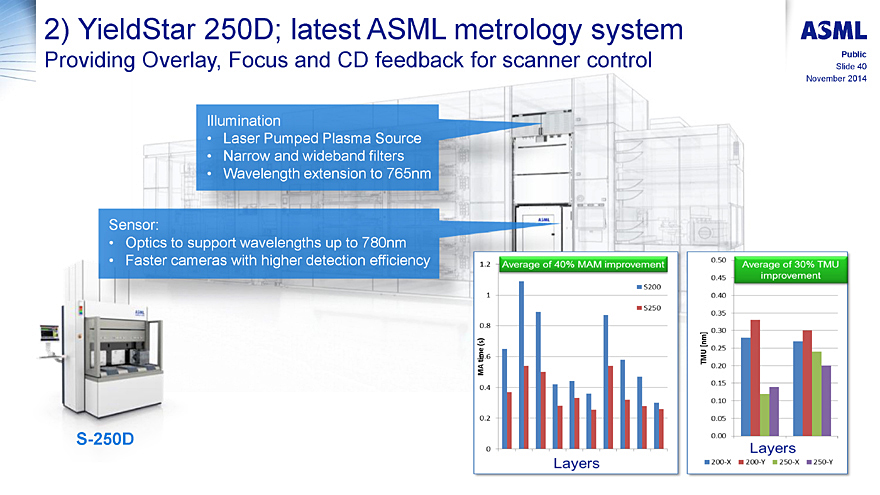
November 2014
2) YieldStar 250D; latest ASML metrology system
Providing Overlay, Focus and CD feedback for scanner control
Illumination
� Laser Pumped Plasma Source
� Narrow and wideband filters
� Wavelength extension to 765nm
Sensor:
� Optics to support wavelengths up to 780nm
� Faster cameras with higher detection efficiency
S-250D
MA time(s)
Average of 40% MAM improvement
1.2
$200
1
$250
0.8
0.6
0.4
0.2
0
Layers
TMU [nm]
Average of 30% TMU improvement
0.50
0.45
0.40
0.35
0.30
0.25
0.20
0.15
0.10
0.05
0.00
Layers
200-X 200-Y 250-X 250-Y
�
ASML
Public
Slide 41
November 2014
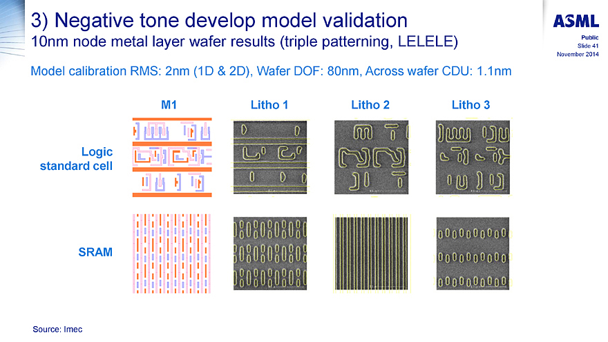
3) Negative tone develop model validation
10nm node metal layer wafer results (triple patterning, LELELE)
Model calibration RMS: 2nm (1D�& 2D), Wafer DOF: 80nm, Across wafer CDU: 1.1nm
M1
Litho 1
Litho 2
Litho 3
Logic standard cell
SRAM
Source: Imec
�
ASML
Public
Slide 42
November 2014
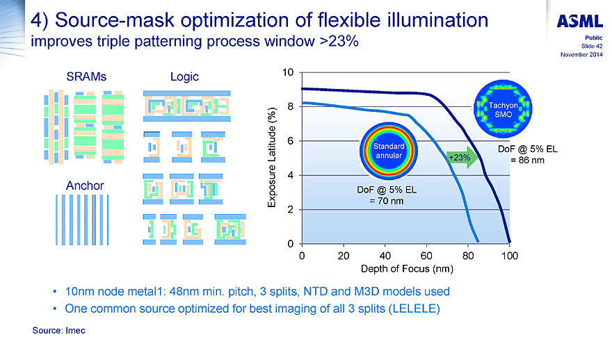
4) Source-mask optimization of flexible illumination improves triple patterning process window >23%
SRAMs
Logic
Anchor
Exposure Latitude (%)
10 8 6 4 2 0
Tachyon SMO
Standard annular
+23%
DoF @ 5% EL
= 86 nm
DoF @ 5% EL
= 70 nm
0
20
40
60
80
100
Depth of Focus (nm)
10nm node metal1: 48nm min. pitch, 3 splits, NTD and M3D models used
One common source optimized for best imaging of all 3 splits (LELELE)
Source: Imec
�
ASML
Public
Slide 43
November 2014
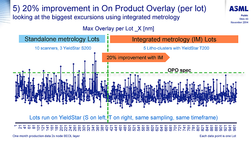
5) 20% improvement in On Product Overlay (per lot) looking at the biggest excursions using integrated metrology
Max Overlay per Lot _X [nm]
Standalone metrology Lots
10 scanners, 3 YieldStar S200
Integrated metrology (IM) Lots
5 Litho-clusters with YieldStar T200
20% improvement with IM
OPO spec
Lots run on YieldStar (S on left, T on right, same sampling, same timeframe)
1 21 41 61 81 101 121 141 161 181 201 221 241 261 281 301 321 341 361 381 401 421 441 461 481 501 521 541 561 581 601 621 641 661 681 701 721 741 761 781 801 821 841 861 881 901 921 941 961
One month production data 2x node BEOL layer
Each data point is one Lot
�
ASML
Public
Slide 44
November 2014
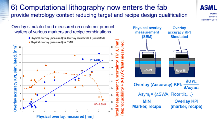
6) Computational lithography now enters the fab provide metrology context reducing target and recipe design qualification
Overlay simulated and measured on customer product wafers of various markers and recipe combinations
� Physical overlay (measured) vs. Overlay accuracy KPI (simulated)
Physical overlay (measured) vs. TMU
Overlay accuracy KPI, simulated, [nm]
16 14 12 10 8 6 4 2 0
R2 = 0.8719
R2 = 0.3914
0.7 0.7 0.6 0.6 0.5 0.5 0.4 0.4 0.3 0.3
0 2 4 6 8 10 12 14 16
Total Measurement Uncertainty, TMU, [nm] (Reproducibility + 0-180� offset) measured,
Physical overlay, measured [nm]
Physical overlay measurement (SEM)
Overlay accuracy KPI Simulated
DSWA
Floor Tilt
Overlay (Accuracy) KPI:
OVL
Asymi
Asymi = {DSWA, Floor tilt,�}
MIN Marker, recipe
Overlay KPI (marker, recipe)
�
ASML
Public
Slide 45
November 2014
ASML enabled 18 moves on the chessboard in 30 years
1973: 1:1 Scanners,
3 um, 75 mm Wafers, 40 Wafers/hr,
5.4 Mpixel/s
1984: G/H line
1,2 um, 100 mm Wafers, 40 W/hr,
61 Mpixel/s
2014: 193 nm Immersion
19 nm, 300 mm Wafers, 250 W/hr,
14 Tpixel/s
1 2 4 8 16 1958 128
256 512 1024 2048 4096 8192 16384 32768
65536 131072 262144 524288 1048576 2097152 1973 8608
16777216 3355443 1984 ASML .34E+08 2.68E+08 5.37E+08 1.07E+09 2.15E+09
4.29E+09 8.59E+09 1.72E+10 3.44E+10 6.87E+10 1.37E+11 2.75E+11 5.5E+11
1.1E+12 2.2E+12 2014 .8E+12 1.76E+13 3.52E+13 7.04E+13 1.41E+14
2.81E+14 5.63E+14 1.13E+15 2.25E+15 4.5E+15 9.01E+15 1.8E+16 3.6E+16 7.21E+16
1.44E+17 2.88E+17 5.76E+17 1.15E+18 2.31E+18 4.61E+18 9.22E+18
Contact printing
1:1 scanners
DUV step scan or expose and repeat
�
ASML
Public
Slide 46
November 2014
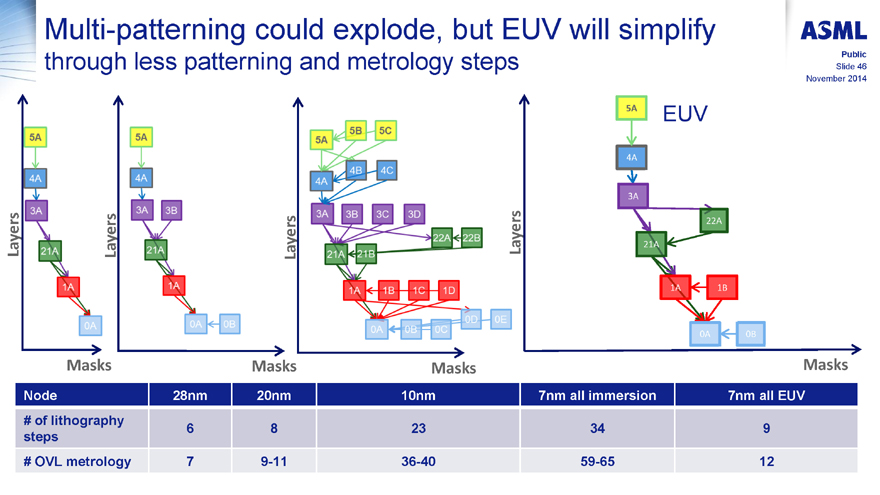
Multi-patterning could explode, but EUV will simplify through less patterning and metrology steps
Layers
5A 4A 3A 21A 1A 0A
Masks
Layers
5A 4A 3A 3B 21A 1A 0A 0B
Masks
Layers
5A 5B 5C
4A 4B 4C
3A 3B 3C 3D
21A 21B 22A 22B
1A 1B 1C 1D
0A 0B 0C 0D 0E
5A 4A 3A 21A 22A 1A 1B 0A 0B
Masks
Layers
EUV
Masks
Node
28nm
20nm
10nm
7nm all immersion
7nm all EUV
# of lithography steps 6 8 23 34 9
# OVL metrology 7 9-11 36-40 59-65 12
�
ASML
Public
Slide 47
November 2014
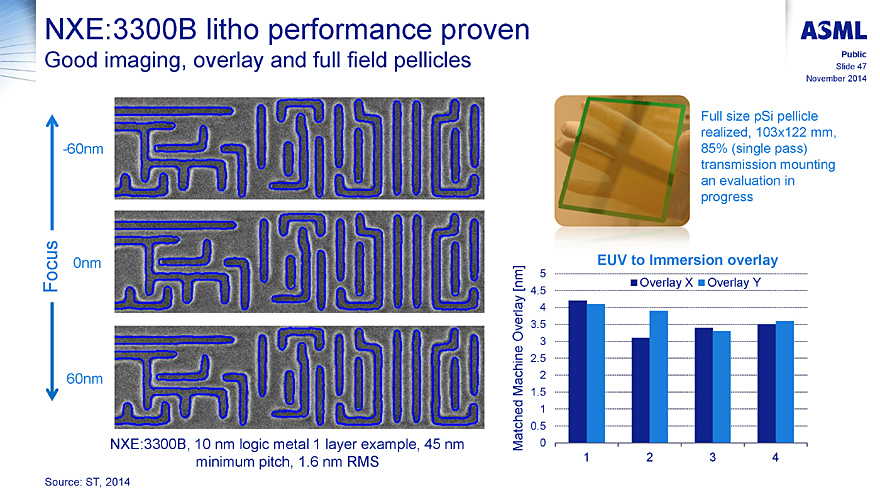
NXE:3300B litho performance proven
Good imaging, overlay and full field pellicles
Focus
-60nm
0nm
60nm
NXE:3300B, 10 nm logic metal 1 layer example, 45 nm minimum pitch, 1.6 nm RMS
Full size pSi pellicle
realized, 103x122 mm,
85% (single pass)
transmission mounting
an evaluation in
progress
Matched Machine Overlay [nm]
5 4.5 4 3.5 3 2.5 2 1.5 1 0.5 0
EUV to Immersion overlay
Overlay X
Overlay Y
1 2 3 4
Source: ST, 2014
�
ASML
Public
Slide 48
November 2014
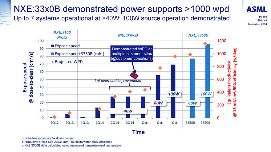
NXE:33x0B demonstrated power supports >1000 wpd
Up to 7 systems operational at >40W; 100W source operation demonstrated
Exposed speed @ dose-to-clear (cm2/s]
100 90 80 70 60 50 40 30 20 10 0
NXE:3100
Proto
Expose speed
Expose speed 3350B (calc.)
Projected WPD
NXE:3300B
Demonstrated WPD at multiple customer sites
(@customer conditions)
Lot overhead improvements
NXE:3350B
40W 80W 100W 80W 100W
1200 1000 800 600 400 200 0
Equivalent Productivity @ 15 mJ/cm2, 50% efficiency [w/day]
2Q12 2Q13 4Q13 1Q14 2Q14 3Q14 Oct. Oct. Oct. 3350B 3350B
Time
o Dose-to-expose is 2.5x dose-to-clear
o Productivity: field size 26x33 mm2, 96 fields/wafer, 50% efficiency
o NXE:3350B data calculated using measured transmission of last system
�
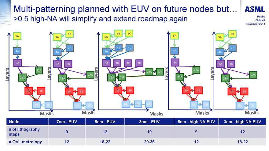
Multi-patterning planned with EUV on future nodes but�
>0.5 high-NA will simplify and extend roadmap again
ASML
Public
Slide 49
November 2014
Layers
5A 4A 3A 22A 21A 1A 1B 0A 0B
Masks
Layers
5B 5A 4B 4A 3A 3B 22A 21A 1A 1B 0A 0B
Masks
Layers
5B 5C 5A 4B 4C 4A 3A 3B 3C 3D 22A 22B 21A 21B 1A 1B 0A 0B 0C
Masks
Layers
5A 4A 3A 22A 21A 1A 1B 0A 0B
Masks
Layers
5B 5A 4B 4A 3A 3B 22A 21A 1A 1B 0A 0B
Masks
Node
7nm - EUV
5nm - EUV
3nm - EUV
5nm - high NA EUV
3nm - high NA EUV
# of lithography steps
9 12 19 9 12
# OVL metrology
12 18-22 29-36 12 18-22
�
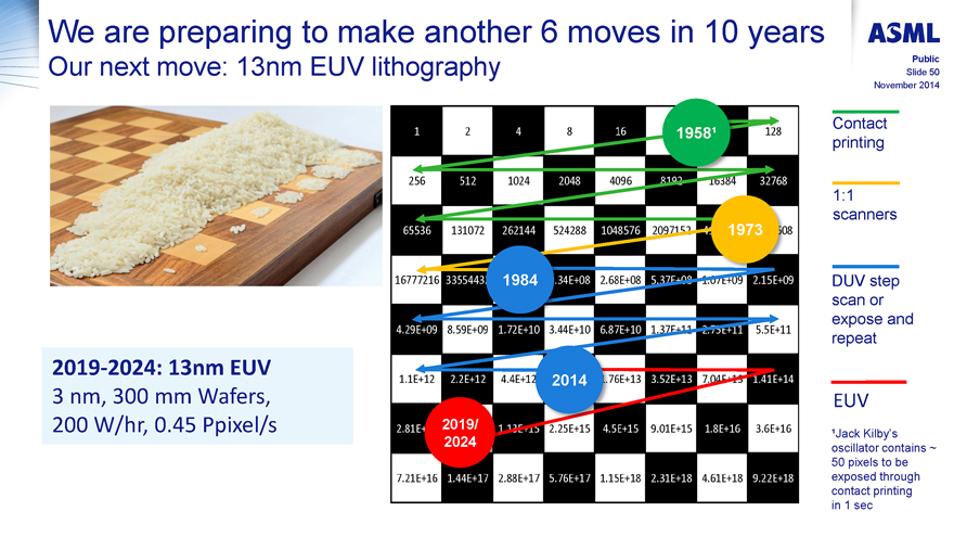
We are preparing to make another 6 moves in 10 years
Our next move: 13nm EUV lithography
ASML
Public
Slide 50
November 2014
2019-2024: 13nm EUV
3 nm, 300 mm Wafers,
200 W/hr, 0.45 Ppixel/s
1 2 4 8 16 128
256 512 1024 2048 4096 8192 16384 32768
65536 131072 262144 524288 1048576 2097152 4 608
16777216 3355443 .34E+08 2.68E+08 5.37E+08 1.07E+09 2.15E+09
4.29E+09 8.59E+09 1.72E+10 3.44E+10 6.87E+10 1.37E+11 2.75E+11 5.5E+11
1.1E+12 2.2E+12 4.4E+12 .76E+13 3.52E+13 7.04E+13 1.41E+14
2.81E+ 1.13E+15 2.25E+15 4.5E+15 9.01E+15 1.8E+16 3.6E+16
7.21E+16 1.44E+17 2.88E+17 5.76E+17 1.15E+18 2.31E+18 4.61E+18 9.22E+18
19581
1973
1984
2014
2019/2024
Contact printing
1:1 scanners
DUV step scan or expose and repeat
EUV
1Jack Kilby�s oscillator contains ~ 50 pixels to be exposed through contact printing in 1 sec
�
Summary
ASML
Public
Slide 51
November 2014
Node progression enabled by immersion multi pass patterning and extended litho metrology and computational litho to control complexity
To address highly complex multi-patterning schemes, EUV insertion is likely at the 10nm logic and 7nm MPU node with full production one node later
ASML has demonstrated consistent EUV source progress. Today performance approaching 100W exposure power. System uptime remains a key challenge
EUV infrastructure supportive for above transition scenarios
Lithography roadmap defined down to the 3nm node
�
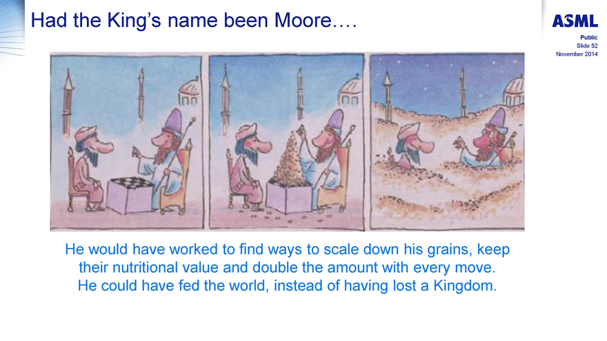
Had the King�s name been Moore�.
ASML
Public
Slide 52
November 2014
He would have worked to find ways to scale down his grains, keep their nutritional value and double the amount with every move.
He could have fed the world, instead of having lost a Kingdom.
�
ASML
INVESTOR DAY
ASMLSMALLTALK2014
LONDON
Exhibit 99.4
�
�
ASML
DUV
Matthew McLaren
Vice President Program Management, DUV
24 November 2014
INVESTOR DAY
ASML SMALLTALK2014
LONDON

�
ASML
Public
Slide 2 November 2014
Forward looking statements
This document contains statements relating to certain projections and business trends that are forward-looking, including statements with respect to our outlook, expected customer demand in specified market segments, expected sales levels and trends, our market share, customer orders and systems backlog, IC unit demand, expected or indicative financial results or targets, including revenue, gross margin, expenses, gross margin percentage, opex percentage of sales, tax percentage, cash conversion cycle, capex percentage of sales, credit rating and earnings per share, expected shipments of tools and the timing thereof, including expected shipments of EUV and DUV tools, productivity of our tools and systems performance, including EUV system performance (such as endurance tests), the development of EUV technology and timing of shipments, development in IC technology, including shrink scenarios, NAND technology development and cost estimates, expectations on development of the shrink roadmap across all of our systems, upgradeability of our tools, system orders, customer transition estimates, expected transition scaling, forecasted industry developments, including expected smartphone, tablet and server use in future years, and expectations relating to new applications including wearable devices and connected devices, expected investment pay-back time for foundries, expected construction of additional holistic lithography infrastructure, the continuation of Moore�s Law, and our dividend policy and intention to repurchase shares. You can generally identify these statements by the use of words like �may�, �will�, �could�, �should�, �project�, �believe�, �anticipate�, �expect�, �plan�, �estimate�, �forecast�, �potential�, �intend�, �continue� and variations of these words or comparable words. These statements are not historical facts, but rather are based on current expectations, estimates, assumptions and projections about the business and our future financial results and readers should not place undue reliance on them.
Forward-looking statements do not guarantee future performance and involve risks and uncertainties. These risks and uncertainties include, without limitation, economic conditions, product demand and semiconductor equipment industry capacity, worldwide demand and manufacturing capacity utilization for semiconductors (the principal product of our customer base), the impact of general economic conditions on consumer confidence and demand for our customers� products, competitive products and pricing, affordability of shrink, the continuation of Moore�s Law, the impact of manufacturing efficiencies and capacity constraints, performance of our systems, the continuing success of technology advances and the related pace of new product development and customer acceptance of new products and customers meeting their own development roadmaps, market demand for our existing products and for new products and our ability to maintain or increase or market share, the development of and customer demand for multi-patterning technology and our ability to meet overlay and patterning requirements, the number and timing of EUV systems expected to be shipped, our ability to enforce patents and protect intellectual property rights, the risk of intellectual property litigation, EUV system performance and customer acceptance, availability of raw materials and critical manufacturing equipment, trade environment, our ability to reduce costs, changes in exchange rates and tax rates, available cash, distributable reserves for dividend payments and share repurchases, changes in our treasury policy, including our dividend and repurchase policy, completion of sales orders, the risk that key assumptions underlying financial targets prove inaccurate, including assumptions relating to market share, lithography market growth and our customers� ability to reduce productions costs, risks associated with Cymer, which we acquired in 2013, and other risks indicated in the risk factors included in ASML�s Annual Report on Form 20-F and other filings with the US Securities and Exchange Commission. These forward-looking statements are made only as of the date of this document. We do not undertake to update or revise the forward-looking statements, whether as a result of new information, future events or otherwise.
�
ASML
Public
Slide 3 November 2014
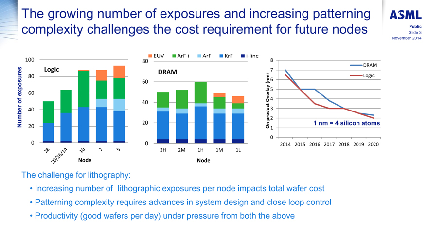
The growing number of exposures and increasing patterning complexity challenges the cost requirement for future nodes
Number of exposures
Logic 100 80 60 40 20 0 28 20/16/2014 10 7 5 Node
EUV ArF-i ArF KrF i-line
DRAM 80 60 40 20 0 2H 2M 1H 1M 1L Node
On product Overlay (nm)
DRAM Logic
8 7 6 5 4 3 2 1 0
1 nm = 4 silicon atoms
2014 2015 2016 2017 2018 2019 2020
The challenge for lithography:
Increasing number of lithographic exposures per node impacts total wafer cost
Patterning complexity requires advances in system design and close loop control
Productivity (good wafers per day) under pressure from both the above
�
ASML
Public
Slide 4 November 2014
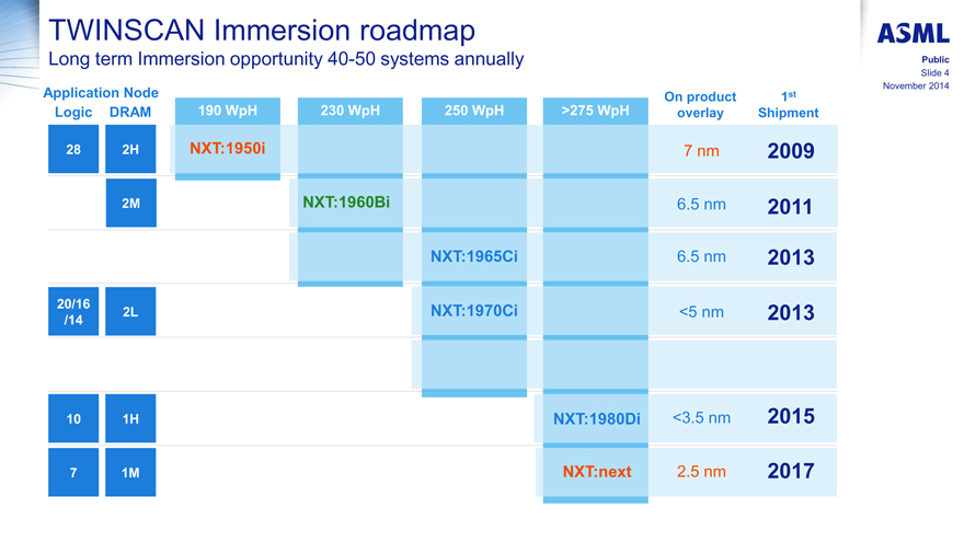
TWINSCAN Immersion roadmap
Long term Immersion opportunity 40-50 systems annually
Application Node Logic DRAM
190 WpH 230 WpH 250 WpH >275 WpH
On product overlay 1st Shipment
28 2H NXT:1950i 7 nm 2009
2M NXT:1960Bi 6.5 nm 2011
NXT:1965Ci 6.5 nm 2013
20/16/14 2L NXT:1970Ci <5 nm 2013
10 1H NXT:1980Di <3.5 nm
2015 7 1M NXT:next 2.5 nm 2017
�
ASML
Public
Slide 5 November 2014
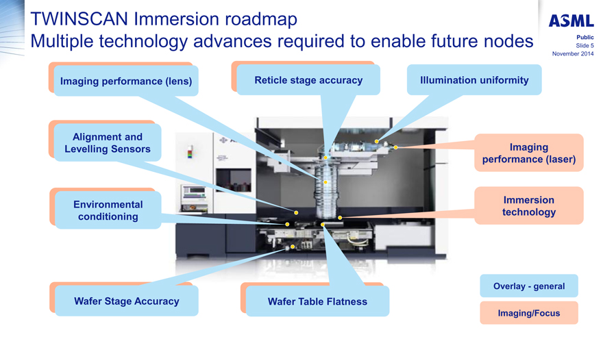
TWINSCAN Immersion roadmap
Multiple technology advances required to enable future nodes
Imaging performance (lens)
Reticle stage accuracy
Illumination uniformity
Alignment and Levelling Sensors
Imaging performance (laser)
Environmental conditioning
Immersion technology
Overlay - general
Wafer Stage Accuracy
Wafer Table Flatness
Imaging/Focus
�
ASML
Public
Slide 6 November 2014
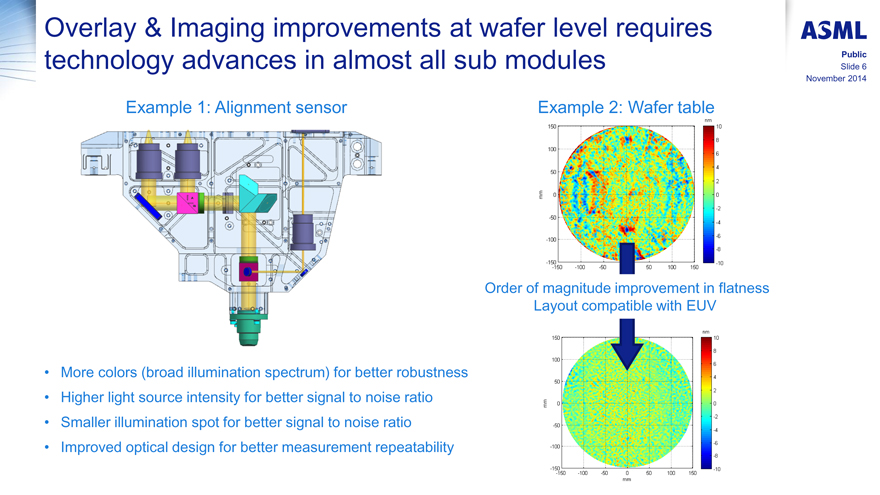
Overlay & Imaging improvements at wafer level requires technology advances in almost all sub modules
Example 1: Alignment sensor
More colors (broad illumination spectrum) for better robustness
Higher light source intensity for better signal to noise ratio
Smaller illumination spot for better signal to noise ratio
Improved optical design for better measurement repeatability
Example 2: Wafer table
mm 150 100 50 0 -50 -100 -150
nm 10 8 6 4 2 0 -2 -4 -6 -8
-150 -100 -50 50 100 150 -10
Order of magnitude improvement in flatness Layout compatible with EUV
mm 150 100 50 0 -50 -100 -150
nm 10 8 6 4 2 0 -2 -4 -6 -8 -10
-150 -100 -50 0 50 100 150 mm
�
ASML
Public
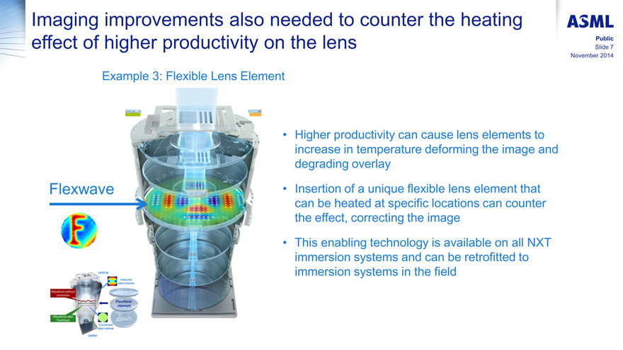
Slide 7 November 2014
Imaging improvements also needed to counter the heating effect of higher productivity on the lens
Example 3: Flexible Lens Element
Flexwave
Higher productivity can cause lens elements to increase in temperature deforming the image and degrading overlay
Insertion of a unique flexible lens element that can be heated at specific locations can counter the effect, correcting the image
This enabling technology is available on all NXT immersion systems and can be retrofitted to immersion systems in the field
�
ASML
Public
Slide 8 November 2014
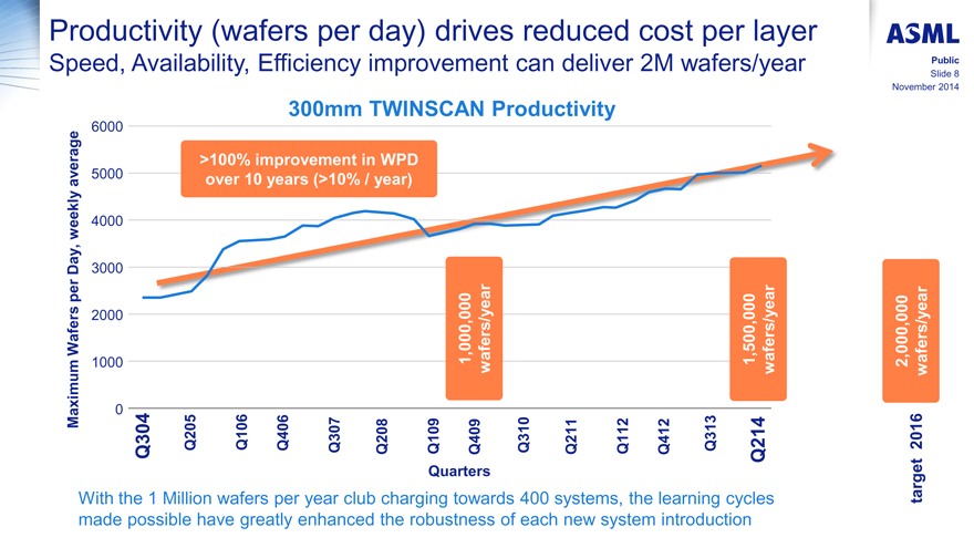
Productivity (wafers per day) drives reduced cost per layer
Speed, Availability, Efficiency improvement can deliver 2M wafers/year
300mm TWINSCAN Productivity
Maximum Wafers per Day, weekly average
6000 5000 4000 3000 2000 1000 0
>100% improvement in WPD over 10 years (>10% / year)
1,000,000 wafers/year
1,500,000 wafers/year
2,000,000 wafers/year
Q304 Q205 Q106 Q406 Q307 Q208 Q109 Q409 Q310 Q211 Q112 Q412 Q313 Q214 Target 2016
With the 1 Million wafers per year club charging towards 400 systems, the learning cycles made possible have greatly enhanced the robustness of each new system introduction
�
ASML
Public
Slide 9
November 2014
TWINSCAN KrF/ArF roadmap: extendibility�& upgradability
Providing lowest Cost of Ownership on the many less critical layer applications
Long term KrF/ArF opportunity 40-55 systems annually
Upgradeable 1st shipment
ArF XT:1450H 7 nm MMO 5 nm MMO
XT:1460K Q2 2015
NA 0.93 +TOP4 option
178 WPH Improved Overlay 205 WPH
KrF XT:1000K 7 nm MMO 5 nm MMO
XT:1060K Q4 2014
NA 0.93 +TOP4 option
205 WPH 205 WPH
KrF XT:860K 7 nm XT:860L 7 nm
Q3 2014
NA 0.80 +TOP4 option 210 WPH Higher +TOP4 option 225 WPH
KrF 20 nm Throughput 20 nm
XT:800K XT:800L Q1 2015
NA 0.80 220 WPH 240 WPH
�
ASML
Public
Slide 10
November 2014
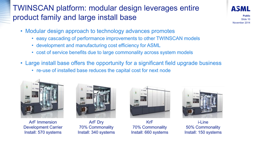
TWINSCAN platform: modular design leverages entire product family and large install base
Modular design approach to technology advances promotes
easy cascading of performance improvements to other TWINSCAN models
development and manufacturing cost efficiency for ASML
cost of service benefits due to large commonality across system models
Large install base offers the opportunity for a significant field upgrade business
re-use of installed base reduces the capital cost for next node
ArF Immersion ArF Dry KrF i-Line
Development Carrier 70% Commonality 70% Commonality 50% Commonality
Install: 570 systems Install: 340 systems Install: 660 systems Install: 150 systems
�
ASML
Public
Slide 11
November 2014
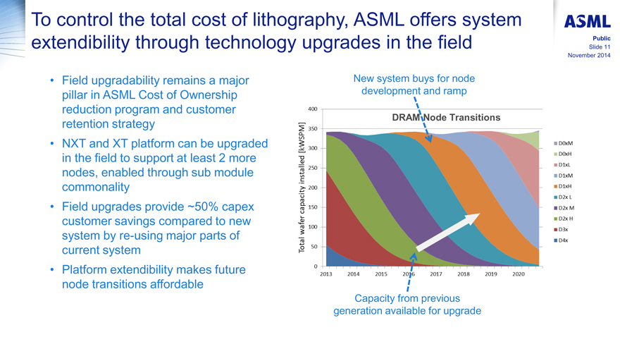
To control the total cost of lithography, ASML offers system extendibility through technology upgrades in the field
Field upgradability remains a major pillar in ASML Cost of Ownership reduction program and customer retention strategy
NXT and XT platform can be upgraded in the field to support at least 2 more nodes, enabled through sub module commonality
Field upgrades provide ~50% capex customer savings compared to new system by re-using major parts of current system
Platform extendibility makes future node transitions affordable
New system buys for node development and ramp
Total wafer capacity installed [kWSPM] 400
350 DRAM Node Transitions D0xM
D0xH
D1xL
300 D1xM
250 D1xH
200 D2x L
150 D2x M
100 D2x H
50 D3x
0 D4x
2013 2014 2015 2016 2017 2018 2019 2020
Capacity from previous generation available for upgrade
�
ASML
Public
Slide 12
November 2014
TWINSCAN Immersion roadmap: System Upgradability
Long term Field Upgrade opportunity ~20 systems annually
Application Node On product 1st
Logic DRAM 190 WpH 230 WpH 250 WpH >275 WpH overlay Shipment
28 2H NXT:1950i 7 nm 2009
2M NXT:1960Bi 6.5 nm 2011
SNEP 1 NXT:1965Ci PEP 275 6.5 nm 2013
20/16 2L NXT:1970Ci PEP 275 <5 nm 2013
/14
SNEP 2
10 1H NXT:1980Di <3.5 nm 2015
SNEP: System Node
Extension Package
7 1M PEP: Productivity NXT:next 2.5 nm 2017
Enhancement Package
�
ASML
Public
Slide 13
November 2014
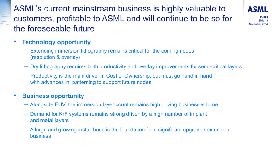
ASML�s current mainstream business is highly valuable to customers, profitable to ASML and will continue to be so for the foreseeable future
Technology opportunity
Extending immersion lithography remains critical for the coming nodes (resolution�& overlay)
Dry lithography requires both productivity and overlay improvements for semi-critical layers
Productivity is the main driver in Cost of Ownership, but must go hand in hand with advances in patterning to support future nodes
Business opportunity
Alongside EUV, the immersion layer count remains high driving business volume
Demand for KrF systems remains strong driven by a high number of implant and metal layers
A large and growing install base is the foundation for a significant upgrade / extension business

�
ASML
INVESTOR DAY
ASMLSMALLTALK2014
LONDON
Exhibit 99.5
�
�
ASML
Holistic Lithography
Christophe Fouquet
Executive Vice President, Applications
24�November 2014
INVESTOR DAY
ASMLSMALLTALK2014
LONDON
�
ASML
Public
Slide 3
November 2014
Holistic Lithography � Introduction
Customer Problem:
Beyond 20nm node scanner and non scanner contributions must be addressed to meet patterning performance requirements
ASML Holistic Lithography:
ASML provides a unique and comprehensive holistic capability via integration of scanner with computational lithography, metrology sensors feeding into scanner knobs to control the process
The scanner is the only manufacturing tool processing and controlling the wafer at field / die level
Customer benefits:
Increased collaboration and technical intimacy with ASML experts�& solutions enable faster and better ramp
Yield is improved, rework�& cycle time are reduced
ASML business opportunity
Holistic lithography revenue opportunity of 1B€ within next 3 years (>20% per year), at very good margins
�
ASML
Public
Slide 4
November 2014
Customer problem: scanner and non scanner contributors to patterning performance must be addressed � example Overlay
Scanner Overlay Error Contribution
NXT-C:1970 NXE:3300
Champion data Champion data
(0.7-0.6nm) (0.9-0.7nm)
99.7%F 99.7%
x: 0.65 nm x: 0.9 nm
10 nm y: 0.56 nm 10 nm y: 0.7 nm
NXT-C:1970�& NXE:3300 - Scanner OVERLAY < 2nm
Other Overlay Error Contributors
wafer 7 10nm
99.7
Max
m+3s
3sd
ovX
42.1
42.1
60.1
59.9
ovY
43.8
43.8
69.7
66.0
Wafer alignment
10nm
Etch fingerprint
IBO pre
5nm
Max
99.7
m+3s
3sd
ovX
7.2
5.2
4.1
4.0
ovY
9.2
5.3
5.1
4.7
CMP fingerprint Metrology accuracy
On product OVERLAY > 6nm
�
ASML
Public
Slide 5
November 2014
ASML holistic lithography: links the scanner to YieldStar metrology and computational lithography design context
NXT - Immersion NXE - EUV
1.Advanced lithography capability
4. Process Window Enlargement 5. Process Window Control Product reticles
3- Computational Lithography Design context 6. Process window detection Product Wafers 2- YieldStar Metrology and Control SW
-1
0
+1
�
ASML
Public
Slide 6
November 2014
Why ASML?: Scanner is the only tool processing and controlling the wafer at field level
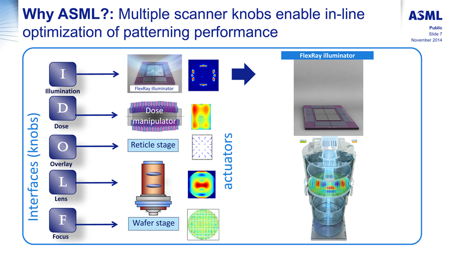
�
ASML
Public
Slide 7
November 2014
Why ASML?: Multiple scanner knobs enable in-line optimization of patterning performance
Interfaces (knobs)
FlexRay illuminator
I
Illumination FlexRay illuminator
D Dose manipulator
Dose
O Reticle stage
Overlay
L actuators
Lens
F Wafer stage
Focus
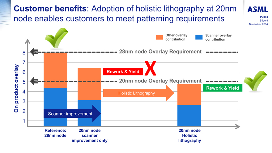
�
ASML
Public
Slide 8
November 2014
Customer benefits: Adoption of holistic lithography at 20nm node enables customers to meet patterning requirements
On product overlay
Other overlay Scanner overlay
contribution contribution
8 L28 28nm node Overlay Requirement
7
6 Rework & Yield X
5 L20 20nm node Overlay Requirement
4 Holistic Lithography Rework & Yield
3
2 Scanner improvement
1
Reference: 28nm node 20nm node scanner improvement only 20nm node Holistic lithography
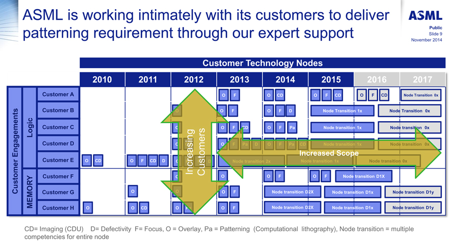
�
ASML
Public
Slide 9
November 2014
ASML is working intimately with its customers to deliver patterning requirement through our expert support
Customer Technology Nodes
2010 2011 2012 2013 2014 2015 2016 2017
Customer A O F O CD O F CD O F CD Node Transition 0x
Customer B O O F O F D Node Transition 1x Node Transition 0x
Logic Customer C O O F CD O F Pa Node transition 1x Node transition 0x
Customer Customer D O CD O F Pa D O F Pa CD Node transition 1x Node transition 0x
Engagements O Pa F D Increased Scope
Customer E O CD O F CD D Increasing Customers Node transition 2x Node transition 1x Node transition 0x
Customer F O O O F O F Node transition D1X
MEMORY Customer G O O O F Node transition D2X Node transition D1x Node transition D1y
Customer H O O CD O Pa O F Node transition D2X Node transition D1x Node transition D1y
CD= Imaging (CDU) D= Defectivity F= Focus, O = Overlay, Pa = Patterning (Computational lithography), Node transition = multiple competencies for entire node
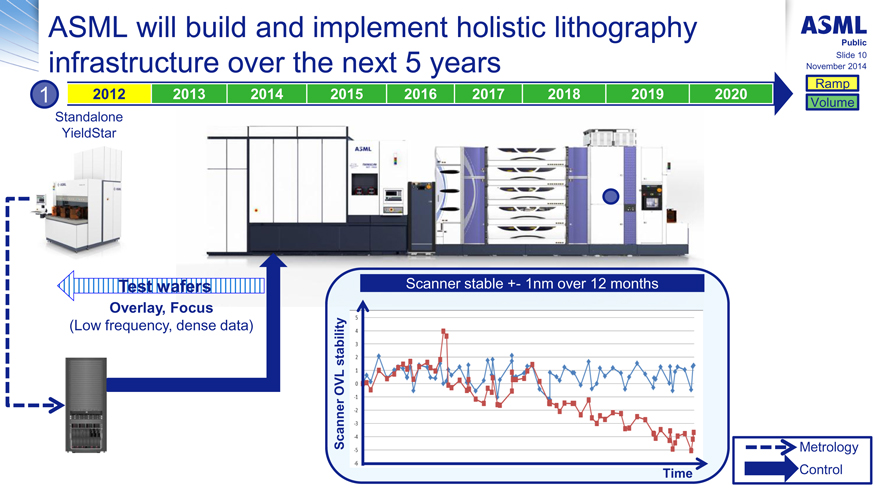
�
ASML
Public
Slide 10
November 2014
ASML will build and implement holistic lithography infrastructure over the next 5 years
1 2012 2013 2014 2015 2016 2017 2018 2019 2020 Ramp Volume
Standalone YieldStar
Test wafers
Overlay, Focus
(Low frequency, dense data)
Scanner stable +- 1nm over 12 months
Scanner OVL stability
5 4 3 2 1 0 -1 -2 -3 -4 -5 -6 Time
Metrology
Control
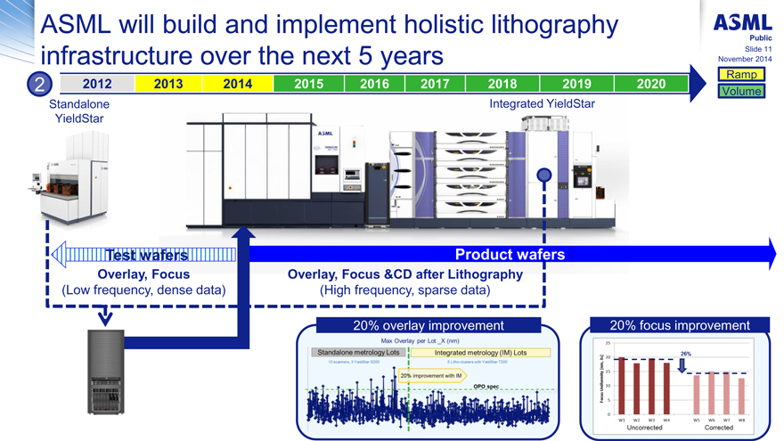
�
ASML
Public
Slide 11
November 2014
ASML will build and implement holistic lithography infrastructure over the next 5 years
2 2012 2013 2014 2015 2016 2017 2018 2019 2020 Ramp Volume
Standalone YieldStar Integrated YieldStar
Test wafers Product wafers
Overlay, Focus (Low frequency, dense data) Overlay, Focus &CD after Lithography (High frequency, sparse data)
20% overlay improvement
Max Overlay per Lot_X (nm)
Standalone metrology Lots
10 scanners, 3 YieldStar S200
Integrated metrology (IM) Lots
5 Litho-clusters with YieldStar T200
20% improvement with IM
OPO spec
20% focus improvement
Focus Uniformity (nm, 3s) 25
20 26%
15
10
5
0
W1 W2 W3 W4 W5 W6 W7 W8
Uncorrected Corrected
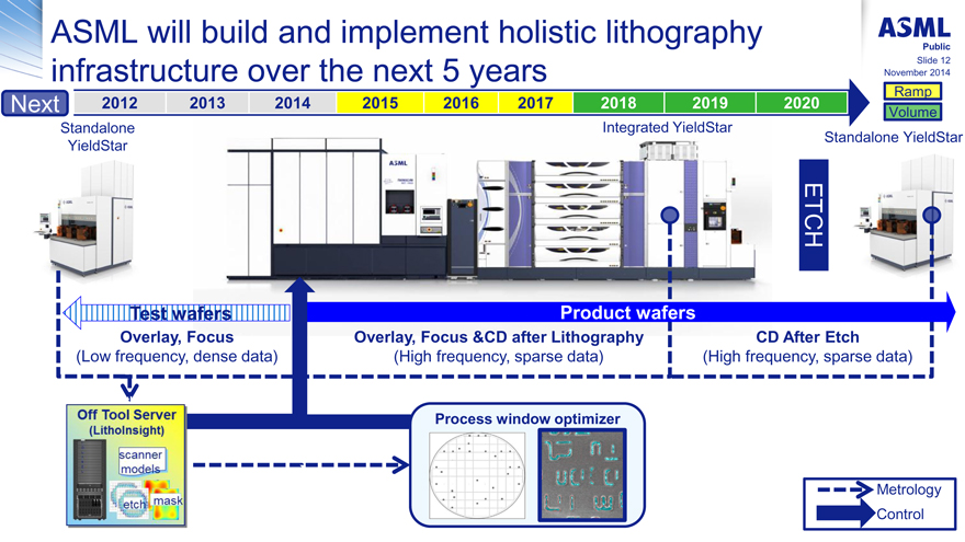
�
ASML
Public
Slide 12
November 2014
ASML will build and implement holistic lithography infrastructure over the next 5 years
Next 2012 2013 2014 2015 2016 2017 2018 2019 2020 Ramp Volume
Standalone YieldStar Integrated YieldStar Standalone YieldStar
ETCH
Test wafers Product wafers
Overlay, Focus (Low frequency, dense data) Overlay, Focus &CD after Lithography (High frequency, sparse data) CD After Etch (High frequency, sparse data)
Off Tool Server (Litholnsight) Process window optimizer
Scanner models
etch mask
Metrology
Control
�
ASML
Public
Slide 13
November 2014
So far: BRION computational lithography continues to extend process window, also using scanners interfaces
ASML
ASML Holistic Lithography TM
Full-chip Source and Mask Optimization
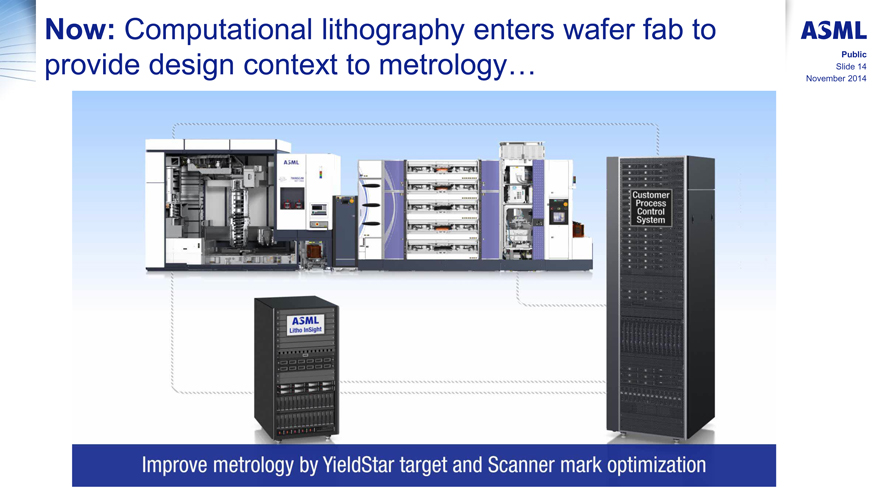
�
ASML
Public
Slide 14
November 2014
Now: Computational lithography enters wafer fab to provide design context to metrology�
ASML
Litho InSight
Customer Process Control System
Improve metrology by YieldStar target and Scanner mark optimization
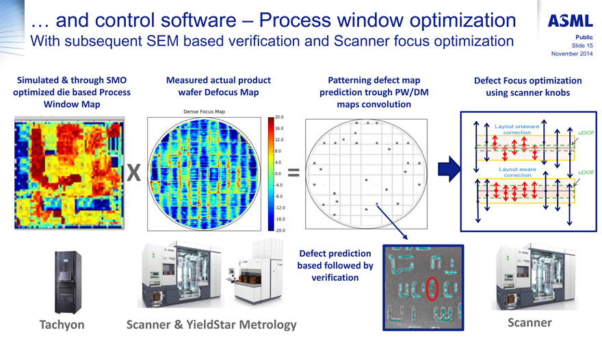
�
ASML
Public
Slide 15
November 2014
� and control software � Process window optimization
With subsequent SEM based verification and Scanner focus optimization
Simulated & through SMO optimized die based Process Window Map
X Tachyon
Measured actual product wafer Defocus Map
Dense Focus Map
20.0 16.0 12.0 8.0 4.0 0.0 -4.0 -8.0 -12.0 -16.0 -20.0
=
Scanner & YieldStar Metrology
Patterning defect map prediction trough PW/DM maps convolution
Defect prediction based followed by verification
Defect Focus optimization using scanner knobs
Layout unaware correction
Layout aware correction
Scanner
uDOF
uDOF
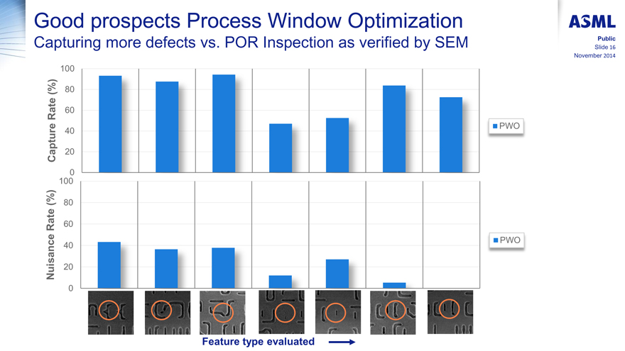
�
ASML
Public
Slide 16
November 2014
Good prospects Process Window Optimization
Capturing more defects vs. POR Inspection as verified by SEM
Capture Rate (%)
100
80
60
40
PWO
20
0
Nuisance Rate (%)
100
80
60
40
PWO
20
0
Feature type evaluated
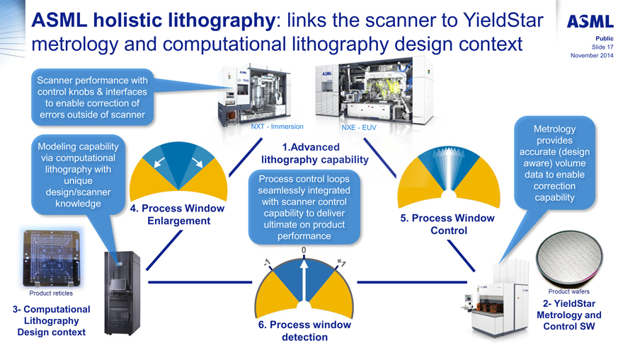
�
ASML
Public
Slide 17
November 2014
ASML holistic lithography: links the scanner to YieldStar metrology and computational lithography design context
Scanner performance with control knobs�& interfaces to enable correction of errors outside of scanner
Modeling capability via computational lithography with unique design/scanner knowledge
Product reticles
3- Computational Lithography Design context
4. Process Window Enlargement
NXT - Immersion
NXE - EUV
1. Advanced lithography capability
Process control loops seamlessly integrated with scanner control capability to deliver ultimate on product performance
6. Process window detection
5. Process Window Control
Metrology provides accurate (design aware) volume data to enable correction capability
Product wafers
2- YieldStar Metrology and Control SW
�
ASML
INVESTOR DAY
ASMLSMALLTALK2014
LONDON
Exhibit 99.6
�
�
�
ASML
EUV
Frits van Hout
Executive Vice President�& Chief Program Officer
24�November 2014
INVESTOR DAY
ASMLSMALLTALK2014
LONDON

�
Forward looking statements
ASML
Public
Slide 2
November 2014
This document contains statements relating to certain projections and business trends that are forward-looking, including statements with respect to our outlook, expected customer demand in specified market segments, expected sales levels and trends, our market share, customer orders and systems backlog, IC unit demand, expected or indicative financial results or targets, including revenue, gross margin, expenses, gross margin percentage, opex percentage of sales, tax percentage, cash conversion cycle, capex percentage of sales, credit rating and earnings per share, expected shipments of tools and the timing thereof, including expected shipments of EUV and DUV tools, productivity of our tools and systems performance, including EUV system performance (such as endurance tests), the development of EUV technology and timing of shipments, development in IC technology, including shrink scenarios, NAND technology development and cost estimates, expectations on development of the shrink roadmap across all of our systems, upgradeability of our tools, system orders, customer transition estimates, expected transition scaling, forecasted industry developments, including expected smartphone, tablet and server use in future years, and expectations relating to new applications including wearable devices and connected devices, expected investment pay-back time for foundries, expected construction of additional holistic lithography infrastructure, the continuation of Moore�s Law, and our dividend policy and intention to repurchase shares. You can generally identify these statements by the use of words like �may�, �will�, �could�, �should�, �project�, �believe�, �anticipate�, �expect�, �plan�, �estimate�, �forecast�, �potential�, �intend�, �continue� and variations of these words or comparable words. These statements are not historical facts, but rather are based on current expectations, estimates, assumptions and projections about the business and our future financial results and readers should not place undue reliance on them.
Forward-looking statements do not guarantee future performance and involve risks and uncertainties. These risks and uncertainties include, without limitation, economic conditions, product demand and semiconductor equipment industry capacity, worldwide demand and manufacturing capacity utilization for semiconductors (the principal product of our customer base), the impact of general economic conditions on consumer confidence and demand for our customers� products, competitive products and pricing, affordability of shrink, the continuation of Moore�s Law, the impact of manufacturing efficiencies and capacity constraints, performance of our systems, the continuing success of technology advances and the related pace of new product development and customer acceptance of new products and customers meeting their own development roadmaps, market demand for our existing products and for new products and our ability to maintain or increase or market share, the development of and customer demand for multi-patterning technology and our ability to meet overlay and patterning requirements, the number and timing of EUV systems expected to be shipped, our ability to enforce patents and protect intellectual property rights, the risk of intellectual property litigation, EUV system performance and customer acceptance, availability of raw materials and critical manufacturing equipment, trade environment, our ability to reduce costs, changes in exchange rates and tax rates, available cash, distributable reserves for dividend payments and share repurchases, changes in our treasury policy, including our dividend and repurchase policy, completion of sales orders, the risk that key assumptions underlying financial targets prove inaccurate, including assumptions relating to market share, lithography market growth and our customers� ability to reduce productions costs, risks associated with Cymer, which we acquired in 2013, and other risks indicated in the risk factors included in ASML�s Annual Report on Form 20-F and other filings with the US Securities and Exchange Commission. These forward-looking statements are made only as of the date of this document. We do not undertake to update or revise the forward-looking statements, whether as a result of new information, future events or otherwise.
�
ASML
Public
Slide 3
November 2014
Outline
New technology transitions: customer perspective
EUV progress�& plans
EUV infrastructure
EUV extendibility
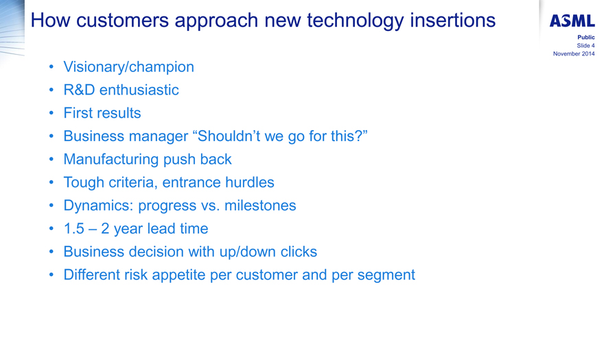
�
How customers approach new technology insertions
ASML
Public
Slide 4
November 2014
Visionary/champion
R&D enthusiastic
First results
Business manager �Shouldn�t we go for this?�
Manufacturing push back
Tough criteria, entrance hurdles
Dynamics: progress vs. milestones
1.5 � 2 year lead time
Business decision with up/down clicks
Different risk appetite per customer and per segment
�
Technology transitions: decisions based on early results
�You have to move to where the puck will be, not where it is� (Wayne Gretzky)
ASML
Public
Slide 5
November 2014
Performance
Decision point
Desired performance at the time of volume ramp
Lead time lengthens due to increasing complexity
Time
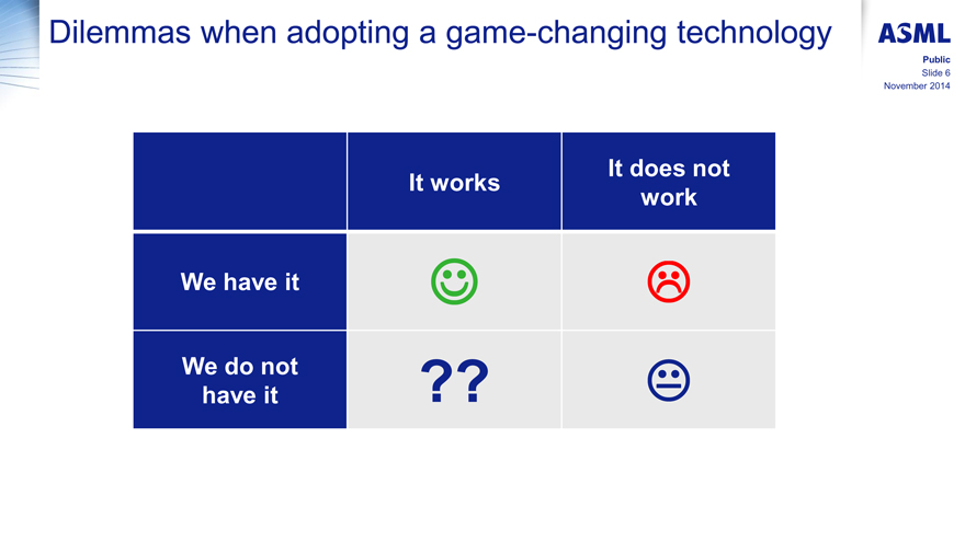
�
Dilemmas when adopting a game-changing technology
ASML
Public
Slide 6
November 2014
It works
It does not work
We have it
We do not have it
�
ASML
Public
Slide 7
November 2014
Outline
New technology transitions: customer perspective
EUV progress�& plans
EUV infrastructure
EUV extendibility
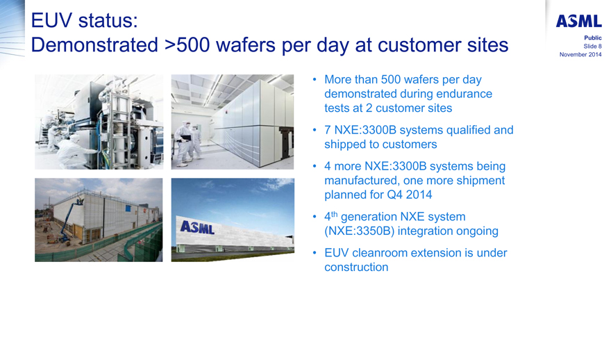
�
EUV status:
Demonstrated >500 wafers per day at customer sites
ASML
Public
Slide 8
November 2014
More than 500 wafers per day demonstrated during endurance tests at 2 customer sites
7 NXE:3300B systems qualified and shipped to customers
4 more NXE:3300B systems being manufactured, one more shipment planned for Q4 2014
4th generation NXE system (NXE:3350B) integration ongoing
EUV cleanroom extension is under construction
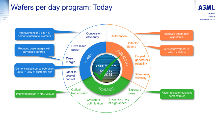
�
Wafers per day program: Today
ASML
Public
Slide 9
November 2014
Improvement of CE to 4% demonstrated at customers
Reduced dose margin with advanced controls
Demonstrated source operation up to ~100W at customer site
Improved design in NXE:3350B
Conversion efficiency
Drive laser power
Dose margin
Laser to droplet control
Optical transmission
Overhead optimization
Stage accuracy at high speed
Exposure dose
Drive laser reliability
Droplet generator reliability
Collector lifetime
Automation
POWER
AVAILABILITY
SCANNER
>500 W ters
per day
2014
Improved automation algorithms
30% improvement in collector lifetime
Faster resist formulations demonstrated
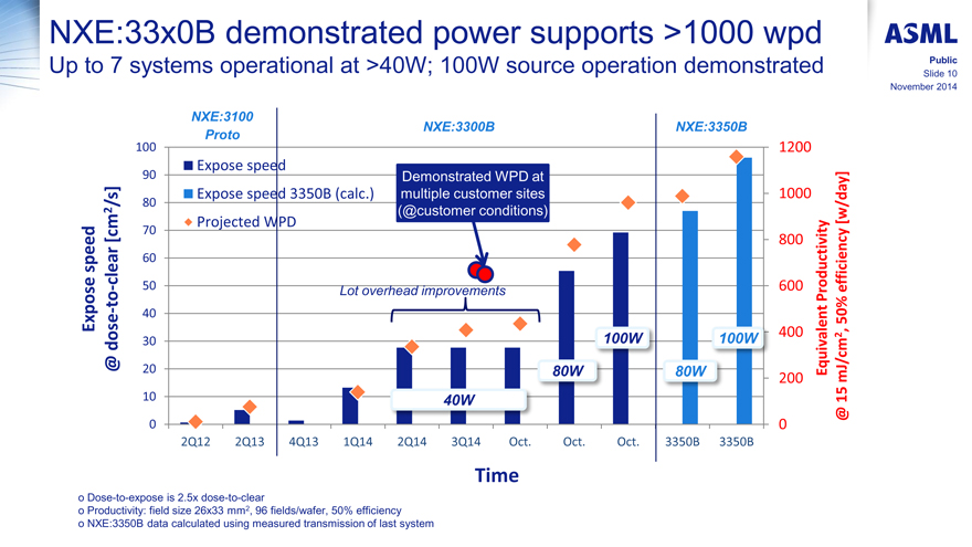
�
NXE:33x0B demonstrated power supports >1000 wpd
Up to 7 systems operational at >40W; 100W source operation demonstrated
ASML
Public
Slide 10
November 2014
Expose speed @ dose-to-clear [cm2/s]
100 90 80 70 60 50 40 30 20 10 0
NXE: 3100
Proto
Expose speed
Expose speed 3350B (calc.)
Projected WPD
NXE:3300B
Demonstrated WPD at multiple customer sites (@customer conditions)
Lot overhead improvements
NXE:3350B
40W
80W
100W
80W
100W
2Q12 2Q13 4Q13 1Q14 2Q14 3Q14 Oct. Oct. Oct. 3350B 3350B
Time
1200 1000 800
600
400
200
0
Equivalent Productivity
@ 15 mJ/cm2, 50% efficiency [w/day]
Dose-to-expose is 2.5x dose-to-clear
Productivity: field size 26x33 mm2, 96 fields/wafer, 50% efficiency
NXE:3350B data calculated using measured transmission of last system
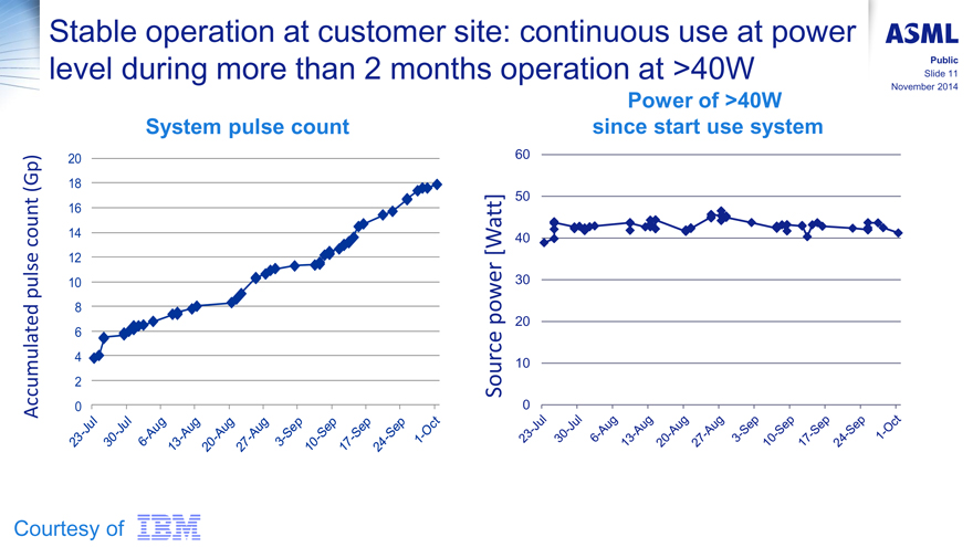
�
Stable operation at customer site: continuous use at power level during more than 2 months operation at >40W
ASML
Public
Slide 11
November 2014
System pulse count
Accumulated pulse count (Gp)
20 18 16 14 12 10 8 6 4
2
0
23-Jul
30-Jul
6-Aug
13-Aug
20-Aug
27-Aug
3-Sep
10-Sep
17-Sep
24-Sep
1-Oct
Power of >40W since start use system
Source power [Watt]
60
50
40 30 20 10
0
23-Jul
30-Jul
6-Aug
13-Aug
20-Aug
27-Aug
3-Sep
10-Sep
17-Sep
24-Sep
1-Oct
Courtesy of IBM
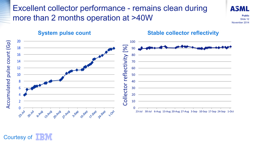
�
Excellent collector performance - remains clean during more than 2 months operation at >40W
ASML
Public
Slide 12
November 2014
System pulse count
Accumulated pulse count (Gp)
20 18 16 14 12 10 8 6 4 2 0
23-Jul
30-Jul
6-Aug
13-Aug
20-Aug
27-Aug
3-Sep
10-Sep
17-Sep
24-Sep
1-Oct
Stable collector reflectivity
Collector reflectivity [%]
100 90 80 70 60 50 40 30 20 10 0
23-Jul 30-Jul 6-Aug 13-Aug 20-Aug 27-Aug 3-Sep 10-Sep 17-Sep 24-Sep 1-Oct
Courtesy of IBM
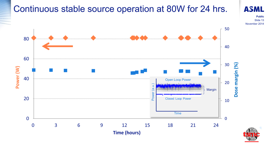
�
Continuous stable source operation at 80W for 24 hrs.
ASML
Public
Slide 13
November 2014
Power (W)
80 60 40 20 0
Power (a.u.)
Open Loop Power
Margin
Closed Loop Power
Time
50
40
30
20
10
0
Dose margin (%)
0 3 6 9 12 15 18 21 24
Time (hours)
tsmc
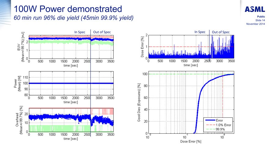
�
100W Power demonstrated
60 min run 96% die yield (45min 99.9% yield)
ASML
Public
Slide 14
November 2014
EUV (Mean+/-99.7%) [mJ]
2
1
0
In Spec
Out of Spec
0
500
1000
1500
2000
2500
3000
3500
time [sec]
Power
(Mean) [W]
110
100
90
80
0
500
1000
1500
2000
2500
3000
3500
time [sec]
Overhead
(Mean+/-99.7%) [%]
20
10
0
0
500
1000
1500
2000
2500
3000
3500
time [sec]
In Spec
Out of Spec
Dose Error [%]
2
1
0
0
500
1000
1500
2000
2500
3000
3500
time [sec]
Good Dies (Exposures) [%]
100
80
60
40
20
0
-2
-1
0
10
10
10
Error
1.0% Error
99.9%
Dose Error [%]
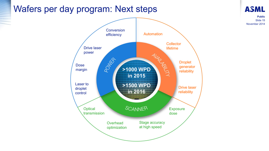
�
Wafers per day program: Next steps
ASML
Public
Slide 15
November 2014
Conversion efficiency
Drive laser power
Dose margin
Laser to droplet control
Optical transmission
Overhead optimization
Stage accuracy at high speed
Exposure dose
Drive laser reliability
Droplet generator reliability
Collector lifetime
Automation
POWER
AVAILABILITY
SCANNER
>1000 WPD
in 2015
>1500 WPD
in 2016
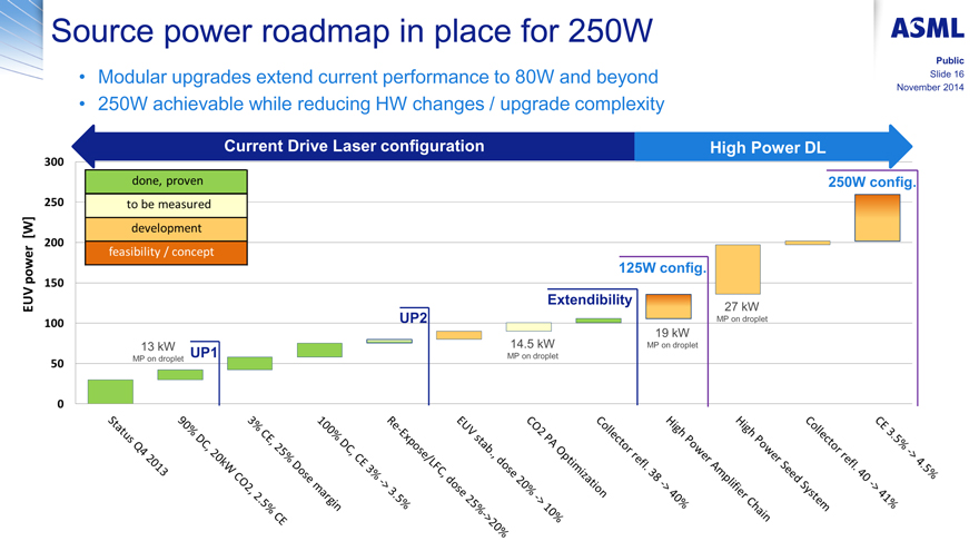
�
Source power roadmap in place for 250W
ASML
Public
Slide 16
November 2014
Modular upgrades extend current performance to 80W and beyond
250W achievable while reducing HW changes / upgrade complexity
Current Drive Laser configuration
High Power DL
EUV power [W]
300
250
200
150
100
50
0
done, proven
to be measured
development
feasibility / concept
13kW
MP on droplet
UP1
UP2
14.5kW
MP on droplet
Extendibility
125W config.
19kW
MP on droplet
27kW
MP on droplet
250W config.
Status Q4 2013
90% DC, 20kW CO2, 2.5% CE
3% CE, 25% Dose margin
100% DC, CE 3% -> 3.5%
Re-Expose/LFC, dose 25%-> 20%
EUV stab., dose 20% -> 10%
CO2 PA Optimization
Collector refl. 38 -> 40%
High Power Amplifier Chain
High Power Seed System
Collector refl. 40 -> 41%
CE 3.5% -> 4.5%
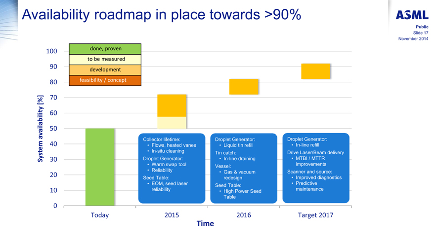
�
Availability roadmap in place towards >90%
ASML
Public
Slide 17
November 2014
System availability [%]
100
90
80
70 60 50 40 30
20
10
0
done, proven
to be measured
development
feasibility / concept
Collector lifetime:
Flows, heated vanes
In-situ cleaning
Droplet Generator:
Warm swap tool
Reliability
Seed Table:
EOM, seed laser reliability
Droplet Generator:
Liquid tin refill
Tin catch:
In-line draining
Vessel:
Gas�& vacuum
redesign
Seed Table:
High Power Seed
Table
Droplet Generator:
In-line refill
Drive Laser/Beam delivery
MTBI / MTTR
improvements
Scanner and source:
Improved diagnostics
Predictive
maintenance
Today 2015 2016 Target 2017
Time
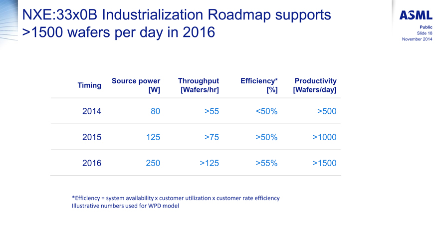
�
NXE:33x0B Industrialization Roadmap supports >1500 wafers per day in 2016
ASML
Public
Slide 18
November 2014
Timing Source power Throughput Efficiency* Productivity
[W] [Wafers/hr] [%] [Wafers/day]
2014 80 >55 <50% >500
2015 125 >75 >50% >1000
2016 250 >125 >55% >1500
*Efficiency = system availability x customer utilization x customer rate efficiency Illustrative numbers used for WPD model
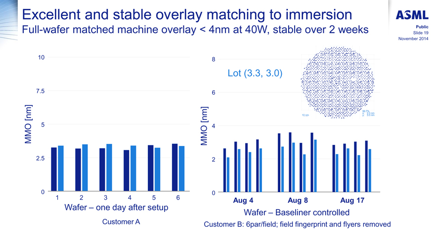
�
Excellent and stable overlay matching to immersion
Full-wafer matched machine overlay < 4nm at 40W, stable over 2 weeks
ASML
Public
Slide 19
November 2014
MMO [nm]
10
7.5
5
2.5
0
1 2 3 4 5 6
Wafer � one day after setup
Customer A
MMO [nm]
8
6
4
2
0
Lot (3.3, 3.0)
10 nm
99.7%
x: 3.3 nm
y: 3.0 nm
Aug 4 Aug 8 Aug 17
Wafer � Baseliner controlled
Customer B: 6par/field; field fingerprint and flyers removed
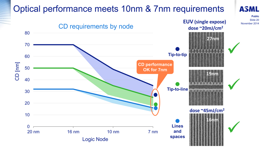
�
Optical performance meets 10nm�& 7nm requirements
ASML
Public
Slide 20
November 2014
CD requirements by node
CD [nm]
80 70 60 50 40 30 20 10 0
CD performance OK for 7nm
20 nm 16 nm 10 nm 7 nm
Logic Node
EUV (single expose)
dose ~20mJ/cm2
Tip-to-tip
27nm
Tip-to-line
19nm
dose ~45mJ/cm2
Lines and spaces
16nm
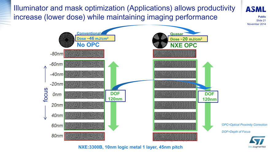
�
Illuminator and mask optimization (Applications) allows productivity increase (lower dose) while maintaining imaging performance
ASML
Public
Slide 21
November 2014
Conventional Dose ~46 mJ/cm2
No OPC
focus
-80nm
-60nm
-40nm
-20nm
0nm
20nm
40nm
60nm
80nm
DOF 120nm
Quasar
Dose ~20 mJ/cm2
NXE OPC
DOF
120nm
OPC=Optical Proximity Correction
DOF=Depth of Focus
NXE:3300B, 10nm logic metal 1 layer, 45nm pitch
ST
life.augmented
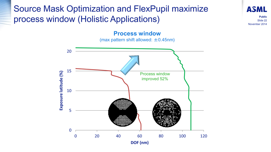
�
Source Mask Optimization and FlexPupil maximize process window (Holistic Applications)
ASML
Public
Slide 22
November 2014
Process window
(max pattern shift allowed: 0.45nm)
Exposure latitude (%)
20
15
10
5
0
Process window improved 52%
0 20 40 60 80 100 120
DOF (nm)
�
ASML
Public
Slide 23
November 2014
Outline
New technology transitions: customer perspective
EUV progress & plans
EUV infrastructure
EUV extendibility
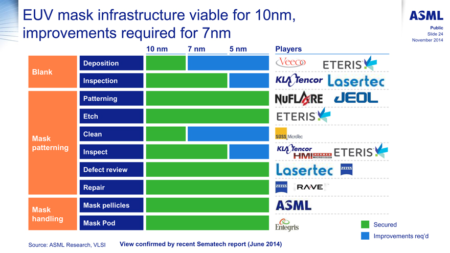
�
EUV mask infrastructure viable for 10nm, improvements required for 7nm
ASML
Public
Slide 24
November 2014
10 nm 7 nm 5 nm Players
Deposition
Blank
Inspection
Patterning
Etch
Mask Clean
patterning Inspect
Defect review
Repair
Mask Mask pellicles
handling Mask Pod
Veeco
KLA Tencor
NUFLARE
ETERISTM
SUSS+MicroTec
KLA Tencor
HMI HERMES MICROVISION
ETERISTM
Lasertec ZEISS
ZEISS RAVE
ASML
Entegris
ETERISTM
Lasertec
JEOL
Secured
Improvements req�d
Source: ASML Research, VLSI
View confirmed by recent Sematech report (June 2014)
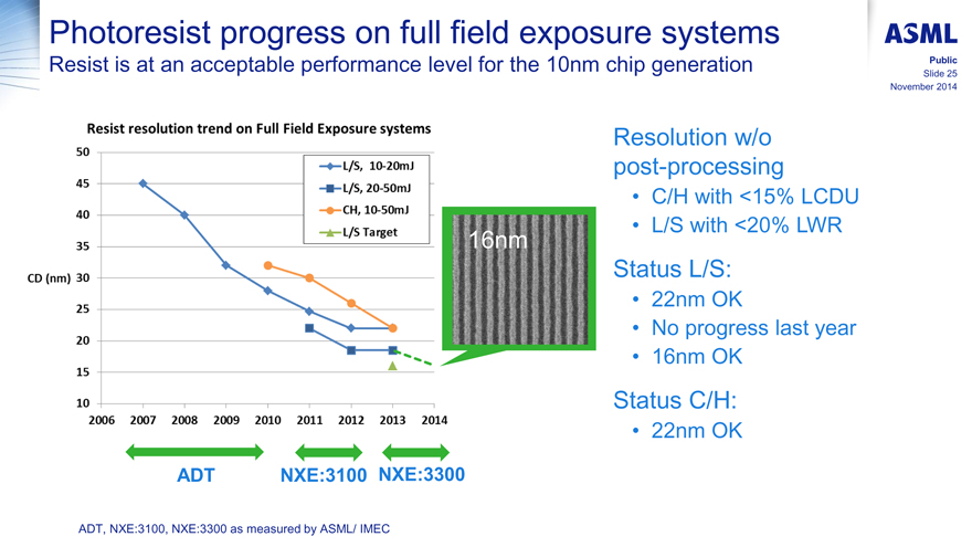
�
Photoresist progress on full field exposure systems
Resist is at an acceptable performance level for the 10nm chip generation
ASML
Public
Slide 25
November 2014
Resist resolution trend on Full Field Exposure systems
CD (nm)
50
45
40
35
30
25
20
15
10
L/S, 10-20mJ
L/S, 20-50mJ
CH, 10-50mJ
L/S Target
16nm
2006
2007
2008
2009
2010
2011
2012
2013
2014
ADT
NXE:3100
NXE:3300
Resolution w/o
post-processing
C/H with <15% LCDU
L/S with <20% LWR
Status L/S:
22nm OK
No progress last year
16nm OK
Status C/H:
22nm OK
ADT, NXE:3100, NXE:3300 as measured by ASML/ IMEC
�
ASML
Public
Slide 26
November 2014
Outline
New technology transitions: customer perspective
EUV progress�& plans
EUV infrastructure
EUV extendibility
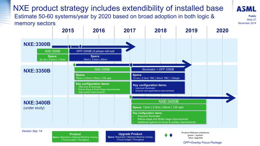
�
NXE product strategy includes extendibility of installed base
Estimate 50-60 systems/year by 2020 based on broad adoption in both logic & memory sectors
ASML
Public
Slide 27
November 2014
2015 2016 2017 2018 2019 2020
NXE:3300B
NXE:3300B
Specs:
22 nm | 5.0nm | 110nm
OFP 3300B (2-phase roll-out)
Specs:
16nm | 3.0nm | 80nm
NXE:3350B
NXE:3350B
Specs:
16nm | 2.5nm | 70nm | 125 wph
Key configuration items:
3350 Lens�& Illuminator
Reticle Stage�& Wafer Stage improvements
Align system improvements
Illuminator + OFP 3350B
Specs:
13 nm | 2.0nm TBC | 60nm TBC | 125wph
Key configuration items:
Improved Illuminator
Scanner and applications improvements
NXE:3400B
(under study)
NXE:3400B
Specs: 13nm | 2.0nm | 60nm | 125 wph
Key configuration items:
Improved Illuminator
Reticle stage and Wafer stage improvements.
Additional options for focus & overlay improvements
Version Sep �14
Product
Specs: Resolution | Matched Machine Overlay
| Focus budget | Throughput
Upgrade Product
Specs: Resolution | Matched Machine Overlay
| Focus budget | Throughput
Product Release milestone green : system blue: upgrade
OFP=Overlay Focus Package
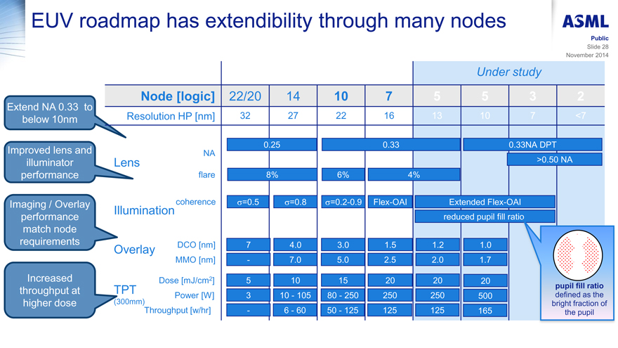
�
EUV roadmap has extendibility through many nodes
ASML
Public
Slide 28
November 2014
Extend NA 0.33 to
below 10nm
Improved lens and illuminator performance
Imaging / Overlay performance match node requirements
Increased throughput at higher dose
Under study
Node [logic] 22/20 14 10 7 5 5 3 2
Resolution HP [nm] 32 27 22 16 13 10 7 <7
0.25 0.33 0.33NA DPT
NA
Lens
>0.50 NA
flare 8% 6% 4%
coherence =0.5 =0.8 =0.2-0.9 Flex-OAI Extended Flex-OAI
Illumination
reduced pupil fill ratio
Overlay
DCO [nm] 7 4.0 3.0 1.5 1.2 1.0
MMO [nm] - 7.0 5.0 2.5 2.0 1.7
Dose [mJ/cm2] 5 10 15 20 20 20
TPT
(300mm)
Power [W] 3 10 - 105 80 - 250 250 250 500
Throughput [w/hr] - 6 - 60 50 - 125 125 125 165
pupil fill ratio defined as the bright fraction of the pupil
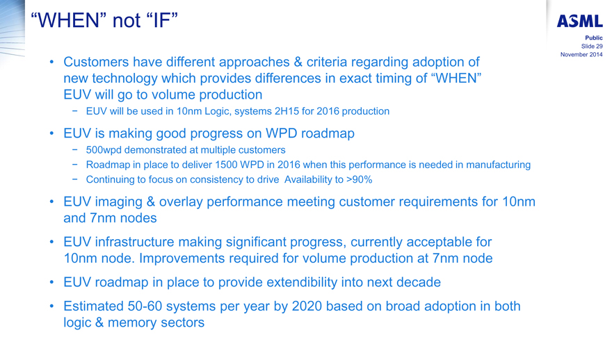
�
�WHEN� not �IF�
ASML
Public
Slide 29
November 2014
Customers have different approaches & criteria regarding adoption of new technology which provides differences in exact timing of �WHEN�
EUV will go to volume production
� EUV will be used in 10nm Logic, systems 2H15 for 2016 production
EUV is making good progress on WPD roadmap
� 500wpd demonstrated at multiple customers
� Roadmap in place to deliver 1500 WPD in 2016 when this performance is needed in manufacturing
� Continuing to focus on consistency to drive Availability to >90%
EUV imaging & overlay performance meeting customer requirements for 10nm and 7nm nodes
EUV infrastructure making significant progress, currently acceptable for 10nm node. Improvements required for volume production at 7nm node
EUV roadmap in place to provide extendibility into next decade
Estimated 50-60 systems per year by 2020 based on broad adoption in both logic & memory sectors

�
ASML
INVESTOR DAY
ASMLSMALLTALK2014
LONDON
Exhibit 99.7
�
Market Update
Peter Jenkins
Vice President, Marketing
24 November 2014
INVESTOR DAY
ASMLSMALLTALK2014
LONDON

�
Forward looking statements
This document contains statements relating to certain projections and business trends that are forward-looking, including statements with respect to our outlook, expected customer demand in specified market segments, expected sales levels and trends, our market share, customer orders and systems backlog, IC unit demand, expected or indicative financial results or targets, including revenue, gross margin, expenses, gross margin percentage, opex percentage of sales, tax percentage, cash conversion cycle, capex percentage of sales, credit rating and earnings per share, expected shipments of tools and the timing thereof, including expected shipments of EUV and DUV tools, productivity of our tools and systems performance, including EUV system performance (such as endurance tests), the development of EUV technology and timing of shipments, development in IC technology, including shrink scenarios, NAND technology development and cost estimates, expectations on development of the shrink roadmap across all of our systems, upgradeability of our tools, system orders, customer transition estimates, expected transition scaling, forecasted industry developments, including expected smartphone, tablet and server use in future years, and expectations relating to new applications including wearable devices and connected devices, expected investment pay-back time for foundries, expected construction of additional holistic lithography infrastructure, the continuation of Moore�s Law, and our dividend policy and intention to repurchase shares. You can generally identify these statements by the use of words like �may�, �will�, �could�, �should�, �project�, �believe�, �anticipate�, �expect�, �plan�, �estimate�, �forecast�, �potential�, �intend�, �continue� and variations of these words or comparable words. These statements are not historical facts, but rather are based on current expectations, estimates, assumptions and projections about the business and our future financial results and readers should not place undue reliance on them.
Forward-looking statements do not guarantee future performance and involve risks and uncertainties. These risks and uncertainties include, without limitation, economic conditions, product demand and semiconductor equipment industry capacity, worldwide demand and manufacturing capacity utilization for semiconductors (the principal product of our customer base), the impact of general economic conditions on consumer confidence and demand for our customers� products, competitive products and pricing, affordability of shrink, the continuation of Moore�s Law, the impact of manufacturing efficiencies and capacity constraints, performance of our systems, the continuing success of technology advances and the related pace of new product development and customer acceptance of new products and customers meeting their own development roadmaps, market demand for our existing products and for new products and our ability to maintain or increase or market share, the development of and customer demand for multi-patterning technology and our ability to meet overlay and patterning requirements, the number and timing of EUV systems expected to be shipped, our ability to enforce patents and protect intellectual property rights, the risk of intellectual property litigation, EUV system performance and customer acceptance, availability of raw materials and critical manufacturing equipment, trade environment, our ability to reduce costs, changes in exchange rates and tax rates, available cash, distributable reserves for dividend payments and share repurchases, changes in our treasury policy, including our dividend and repurchase policy, completion of sales orders, the risk that key assumptions underlying financial targets prove inaccurate, including assumptions relating to market share, lithography market growth and our customers� ability to reduce productions costs, risks associated with Cymer, which we acquired in 2013, and other risks indicated in the risk factors included in ASML�s Annual Report on Form 20-F and other filings with the US Securities and Exchange Commission. These forward-looking statements are made only as of the date of this document. We do not undertake to update or revise the forward-looking statements, whether as a result of new information, future events or otherwise.
ASML Public Slide 2 November 2014
�
ASML
Public
Slide 3
November 2014
Outline
Introduction
ASML value drivers
Market opportunity & affordability
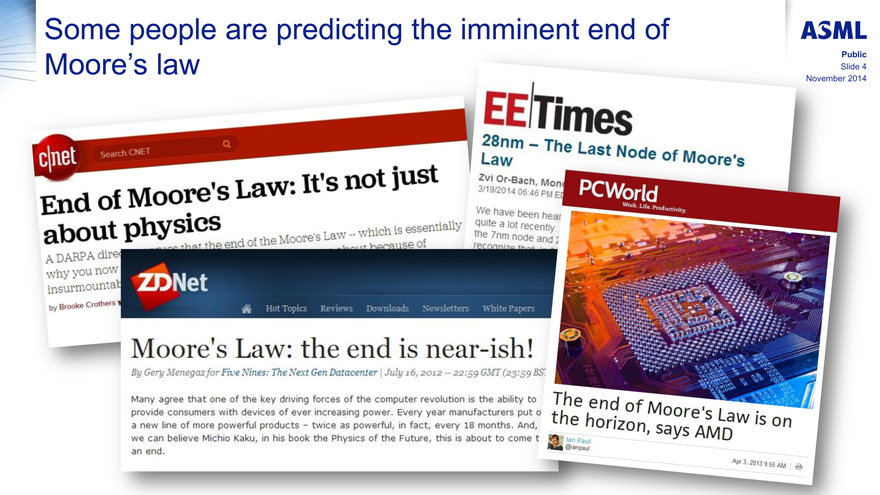
�
ASML
Public
Slide 4
November 2014
Some people are predicting the imminent end to Moore�s law
c|net Search CNET
End of Moore� Law: It�s not just about physics
A DARPA dire that the end of the Moore�s Law -- which is essentially why you now because of insurmountab
by Brooke Crothers
EE|Times
28nm -- The Last Node of Moore�s Law
Zvi Or-Bach, Mon
3/19/2014 06:46 PM ED
We have been hear quite a lot recently. the 7nm node and 2 recognize
ZDnet
Hot Topics Reviews Downloads Newspapers White Papers
Moore�s Law: the end is near-ish!
By Gear Menegaz for Five Nines: The Next Gen Datacenter | July 16, 2012 -- 22:59 GMT (23:59 BST
Many agree that one of the key driving forces of the computer revolution is the ability to provide consumers with devices of ever increasing power. Every year manufacturers put o a new line of more powerful products - twice as powerful, in fact, every 18 months. And, we can believe Michio Kaku, in his book the Physics of the Future, this is about to come t an end.
PCWorld Work. Life. Productivity.
The end of Moore�s Law is on the horizon, says AMD
Ian Paul
@ianpaul Apr 3, 2013 9:55 AM
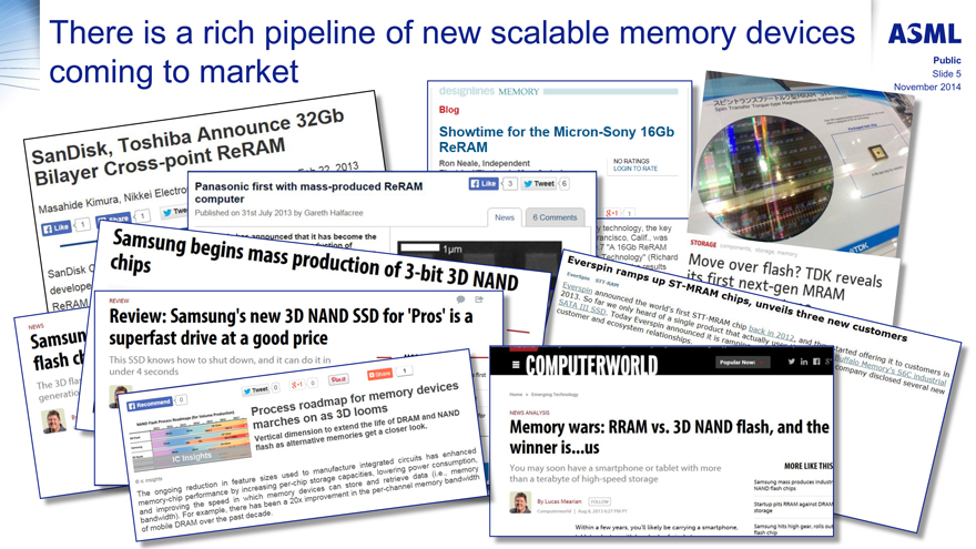
�
There is a rich pipeline of new scalable memory devices coming to market
ASML
Public
Slide 5
November 2014
SanDisk, Toshiba Announce 32Gb Bilayer Cross-point ReRAM
Masahide Kimura, Nikkei Electro 2013
f Like 1 Share 1 Twe
SanDisk
develope
ReRAM
designlines MEMORY
Blog
Showtime for the Micron-Sony 16Gb ReRAM
Ron Neale, Independent
No Ratings
LOGIN TO RATE
g+1 1
y technology, the key
rancisco, Calif., was
.7 �A 16Gb ReRAM
Technology� (Richard
results
MRAM STT-MRAM
Spin Transfer Torque-type Magnetoresistive Random Access Memory
TDK
STORAGE components, storage, memory
Move over flash? TDK reveals its first next-gen MRAM
Panasonic first with mass-produced ReRAM computer f Like 3 Tweet 6
Published on 31st July 2013 by Gareth Halfacree News 6 Comments
announced that it has become the
of 1 m
NEWS
Samsun
flash
The 3D fla
generatio
Samsung begins mass production of 3-bit 3D NAND chips
REVIEW
Review: Samsung�s new 3D NAND SSD for �Pros� is a superfast drive at a good price
This SSD knows how to shut down, and it can do it in under 4 seconds
f Recommend 0 Tweet 0 g+1 0 Pin it +Share 1
NAND Flash Process Roadmaps (for Volume Production)
2011 2012 2013 2014 2015 2016 2017
IC Insights
Process roadmap for memory devices marches on as 3D looms
Vertical dimension to extend the life of DRAM and NAND flash as alternative memories get a closer look.
C ic insights
The ongoing reduction in feature sizes used to manufacture integrated circuits has enhanced memory-chip performance by increasing per-chip storage capacities, lowering power consumption, and improving the speed in which memory devices can store and retrieve data (i.e., memory bandwidth). For example, there has been a 20x improvement in the per-channel memory bandwidth of mobile DRAM over the past decade.
Everspin ramps up ST-MRAM chips, unveils three new customers
EverSpin STT-RAM
Everspin announced the world�s first STT-MRAM chip back in 2012, and they started offering it to customers in 2013. So far we only heard of a single product that actually uses Buffalo Memory�s S6C industrial SATA III SSD. Today Everspin announced it is ram company disclosed several new customer and ecosystem relationships.
COMPUTERWORLD Popular Now: in f g+
Home > Emerging Technology
NEWS ANALYSIS
Memory wars: RRAM vs. 3D NAND flash, and the winners is...us
You may soon have smartphone or tablet with more than a terabyte of high-speed storage
By Lucas Mearian FOLLOW
Computerworld | Aug 8, 2013 6:27 PM PT
Within a few years, you�ll likely be carrying a smartphone,
MORE LIKE THIS
Samsung mass produces industr
NAND flash Chips
Startup pits RRAM against DRAM
storage
Samsung hits high gear, rolls out flash chip
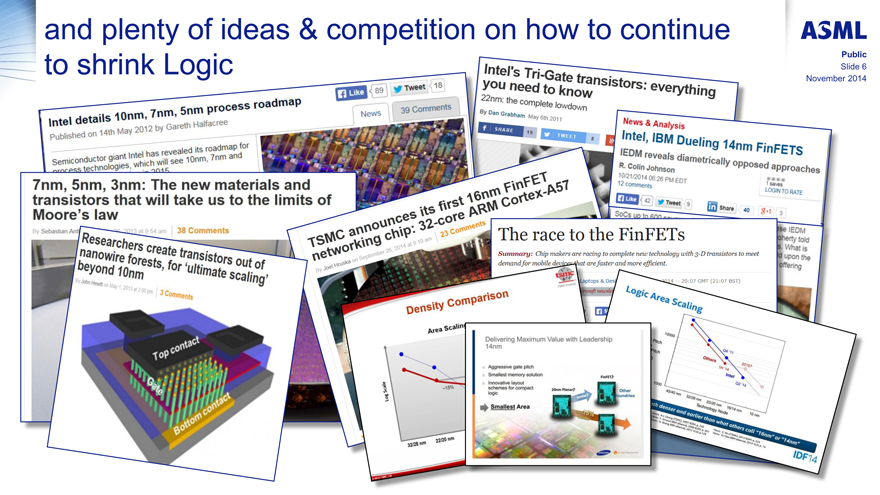
�
ASML
Public
Slide 6
November 2014
and plenty of ideas & competition on how to continue to shrink Logic
Intel details 10nm, 7nm, 5nm process roadmap
Published on 14th May 2012 by Gareth Haltafacre
f Like 89 Tweet 18
News 39 Comments
Semiconductor giant Intel has revealed its roadmap for process technologies, which will see 10nm, 7nm and
7nm, 5nm, 3nm: The new materials and transistors that will take us to the limits of Moore�s law
By Sebastian Anth 2013 at 9:54 am | 38 comments
Researchers create transistors out of nanowire forests, for �ultimate scaling� beyond 10nm
By John Hewitt on May 1, 2013 at 2:00 pm | 3 Comments
Top contact Gate Bottom contact
TSMC announces its first 16nm FinFET networking chip: 32-core ARM Cortex-A57
By Joel Hruska on September 26, 2014 at 9:10 am | 23 comments
Density Comparison tsmc TSMC Property
Area Scaling
Log Scale
~15% 32/28 nm 22/20 nm
Intel�s Tri-Gate transistors: everything you need to know
22nm: the complete lowdown
By Dan Grabham May 6th 2011
f SHARE 19 TWEET 8 g+
News & Analysis
Intel, IBM Dueling 14nm FinFETS
IEDM reveals diametrically opposed approaches
R. Colin Johnson
10/21/2014 06:26 PM EDT
12 comments
f Like 42 Tweet 9 in share 40 g+1 3
1 saves LOGIN TO RATE
SoCs up to 600 ese IEDM oherty told s. What is d upon the offering
The race to the FinFETs
Summary: Chip makers are racing to complete new technology with 3-D transistors to meet demand for mobile device that are faster and more efficient.
Laptops & Des 2014 -- 20:07 GMT (21:07 BST) crosoft newslet f S
Logic Area Scaling 10000 Pitch Pitch Q4�11 Others 1H�14 Intel Q2�14 2015?
1000 45/40 nm 32/28 nm 22/20 nm 16/14 nm 10 nm Technology Node
th denser and earlier than what others call �16nm� or �14nm�
45nm: K-L Cheng (TSMC), 2007 IEDM, p. 243
28nm: F. Arnaud (IBM alliance), 2009 IEDM, p. 651
0nm: H. Shang (IBM alliance), 2012 VLSL p. 129
16nm: S. Wu (TSMC), 2013 IEDM, p. 224
10nm: K-1 Seo (IBM alliance), 2014 VLSL, p. 14 IDF14
Delivering Maximum Value with Leadership 14nm
Agrresive gate pitch
Smallest memory solution
Innovative layout schemes for compact logic 20nm Planar FinFET Other foundries Similar up to 15% Smaller
Smallest Area
Samsung
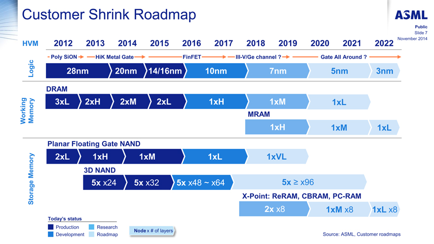
�
ASML
Public
Slide 7
November 2014
Customer Shrink Roadmap
HVM 2012 2013 2014 2015 2016 2017 2018 2019 2020 2021 2022
Poly SiON Hik Metal Gate FinFet III-V/Ge channel ? Gate All Around ?
Logic 28nm 20nm 14/16nm 10nm 7nm 5nm 3nm
DRAM
Working Memory 3xL 2xH 2xM 2xL 1xH 1xM 1xL
MRAM
1xH 1xM 1xl
Planar Floating Gate NAND
Storage Memory 2xL 1xH 1xM 1xL 1xVL
3D NAND
5x x24 5x x32 5x x48 ~ x64 5x � x96
X-Point: ReRAM, CBRAM, PC-RAM
2x 28 1xM x8 1xL x8
Today�s status
Production Research
Development Roadmap
Node x # of layers
Source: ASML, Customer roadmaps
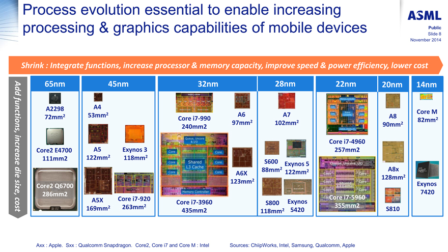
�
Process evolution essential to enable increasing processing & graphics capabilities of mobile devices
ASML
Public
Slide 8
November 2014
Shrink : Integrate functions, increase processor & memory capacity, improve speed & power efficiency, lower cost
Add functions, increase die size, cost
65nm 45nm 32nm 28nm 22nm 20nm 14nm
A2298 72mm2 Core2 E4700 111mm2 Core2 Q6700 286mm2
A4 53mm2 A5 122mm2 Exynos 3 118mm2 A5X 169mm2 Core i7-920 263mm2
Core i7-990 240mm2 A6 97mm2 Queue, Uncore & I/O Core Core Core Shared L3 Cache Core Core Core Memory Controller A6X 123mm2 Core i7-3960 435mm2
A7 102mm2 S600 88mm2 Exynos 5 122mm2 S800 118mm2 Exynos 5420
Core i7-4960 257mm2 Queue, Uncore, I/O Core Core Core Core Shared L3 Cache Core Core Core Core i7-5960 355mm2
A8 90mm2 A8x 128mm2 S810
Core M 82mm2 Exynos 7420
Axx : Apple. Sxx : Qualcomm Snapdragon. Core2, Core i7 and Core M : Intel Sources: ChiipWorks, Intel, Samsung, Qualcomm, Apple
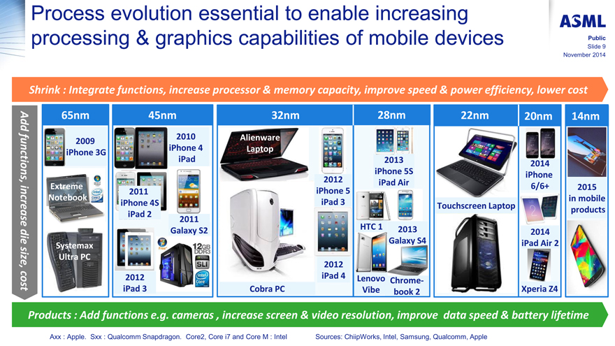
�
Process evolution essential to enable increasing processing & graphics capabilities of mobile devices
ASML
Public
Slide 9
November 2014
Shrink: Integrate functions, increase processor & memory capacity, improve speed & power efficiency, lower cost
Add functions, increase die size, cost
65nm 45nm 32nm 28nm 22nm 20nm 14nm
2009 iPhone 3G
Extreme Notebook
Windows
intel Core 2 Quad
Systemax Ultra PC
2010 iPhone 4 iPad
2011 iPhone 4S iPad 2
2011 Galaxy S2
2012 iPad 3
7 free
12GB DDR3
NVIDIA SLI
intel Core 17
Alienware Laptop
2012 iPhone 5 iPad 3
Cobra PC
2012 iPad 4
2013 iPhone 5S iPad Air
HTC 1
2013 Galaxy S4
Lenovo Vibe
Chrome-book 2
Touchscreen Laptop
2014 iPhone 6/6+
2014 iPad Air 2
Xperia Z4
2015 in mobile products
Products: Add functions e.g. cameras, increase screen & video resolution, improve data speed & battery lifetime
Axx : Apple. Sxx : Qualcomm Snapdragon. Core2, Core i7 and Core M : Intel Sources: ChiipWorks, Intel, Samsung, Qualcomm, Apple
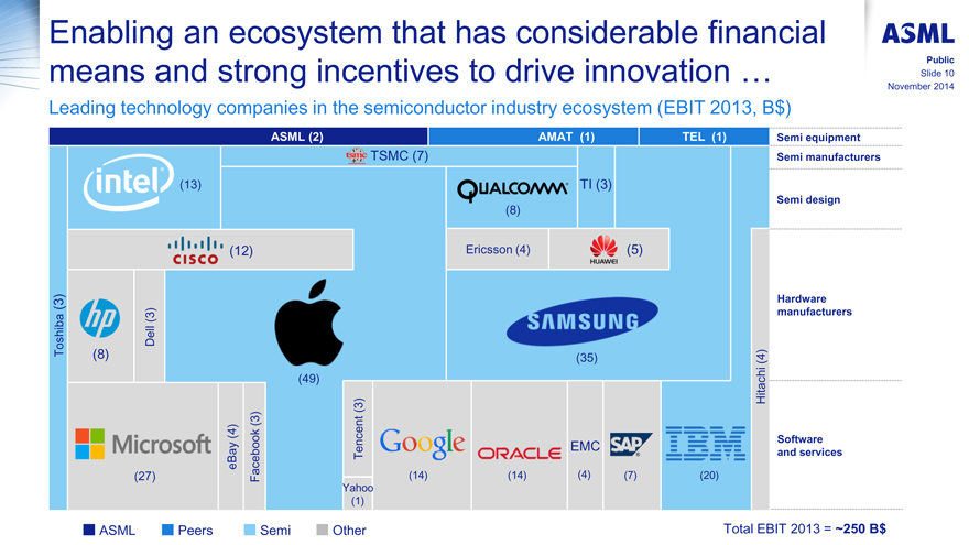
�
ASML
Public
Slide 10
November 2014
Enabling an ecosystem that has considerable financial means and strong incentives to drive innovation ...
Leading technology companies in the semiconductor industry ecosystem (EBIT 2013, B$)
ASML (2) AMAT (1) TEL (1)
TSMC (7)
intel (13) QUALCOMM� (8) TI (3)
Semi equipment
Semi manufacturers
Semi design
CISCO (12) Ericsson (4) HUAWEI (5)
Toshiba (3) HP (8) Dell (3) (49) SAMSUNG (35) Hitachi (4)
Hardware manufacturers
Microsoft (27) eBay (4) Facebook (3) Yahoo (1) Tencent (3) Google (14) ORACLE (14) EMC (4) SAP� (7) IBM (20)
Software and services
ASML Peers Semi Other
Total EBIT 2013 = ~250 B$
�
ASML
Public
Slide 11
November 2014
Outline
Introduction
ASML value drivers
Market opportunity�& affordability
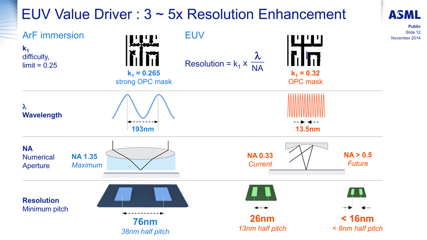
�
ASML
Public
Slide 12
November 2014
EUV Value Driver : 3 ~ 5x Resolution Enhancement
ArF immersion EUV
k1 difficulty,
limit = 0.25 Resolution = k1 x NA
k1 = 0.265 k1 = 0.32
strong OPC mask OPC mask
Wavelength
193nm 13.5nm
NA
Numerical NA 1.35 NA 0.33 NA > 0.5
Aperture Maximum Current Future
Resolution
Minimum pitch
76nm 26nm < 16nm
38nm half pitch 13nm half pitch < 8nm half pitch
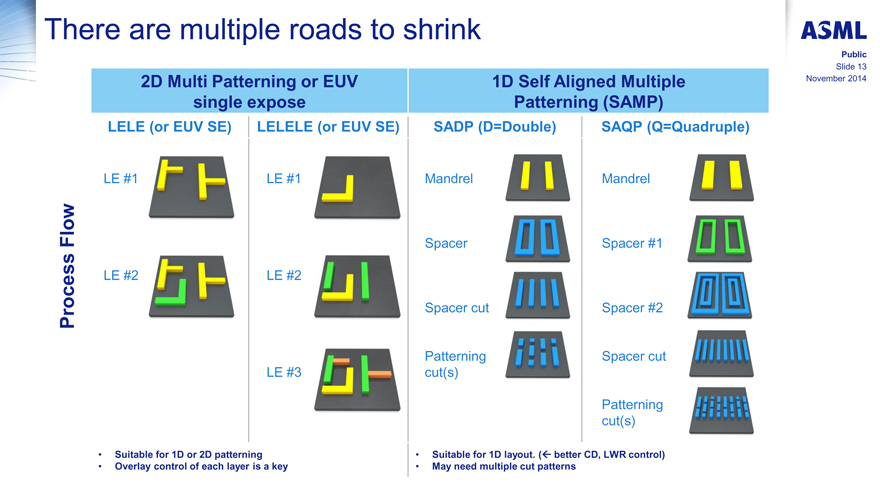
�
ASML
Public
Slide 13
November 2014
There are multiple roads to shrink
Process Flow
2D Multi Patterning or EUV single expose 1D Self Aligned Multiple Patterning (SAMP)
LELE (or EUV SE) LELELE (or EUV SE) SADP (D=Double) SAQP (Q=Quadruple)
LE #1 LE #1 Mandrel Mandrel
Spacer Spacer #1
LE #2 LE #2
Spacer cut Spacer #2
LE #3 Patterning cut(s) Spacer cut
Patterning cut(s)
Suitable for 1D or 2D patterning
Overlay control of each layer is a key
Suitable for 1D layout. (better CD, LWR control)
May need multiple cut patterns
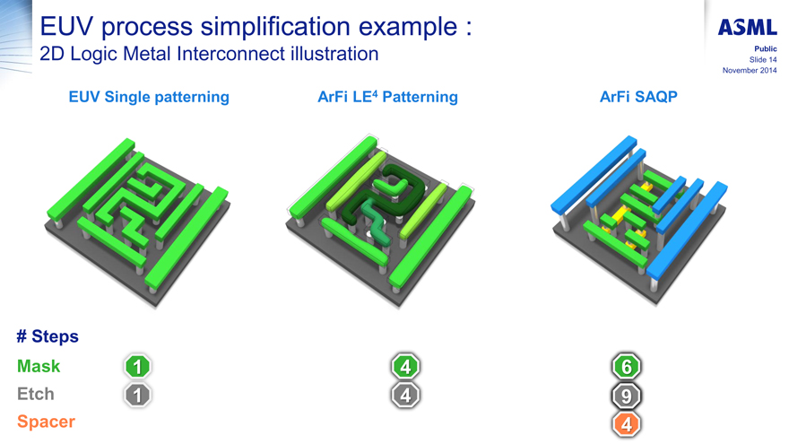
�
ASML
Public
Slide 14
November 2014
EUV process simplification example :
2D Logic Metal Interconnect illustration
EUV Single patterning ArFi LE4 Patterning ArFi SAQP
# Steps
Mask 1 4 6
Etch 1 4 9
Spacer 4
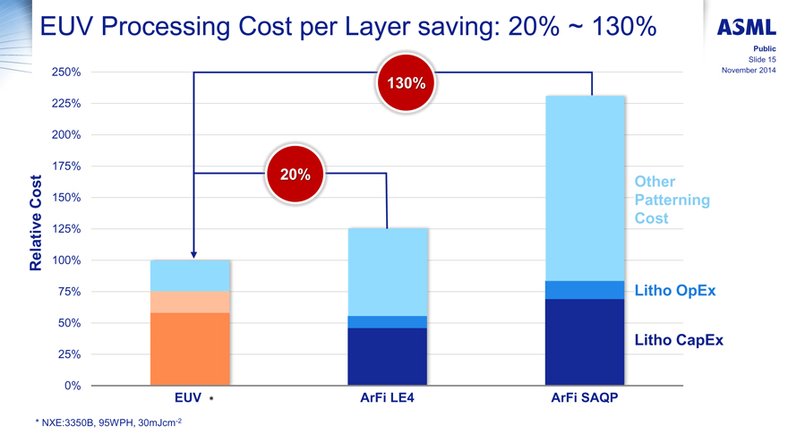
�
ASML
Public
Slide 15
November 2014
EUV Processing Cost per Layer saving: 20% ~ 130%
Relative Cost
250%
225%
200%
175%
150%
125%
100%
75%
50%
25%
0%
130%
20%
Other Patterning Cost
Litho OpEx
Litho CapEx
EUV * ArFi LE4 ArFi SAQP
* NXE:3350B, 95WPH, 30mJcm-2
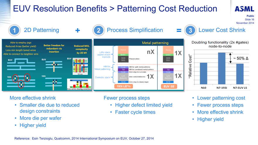
�
ASML
Public
Slide 16
November 2014
EUV Resolution Benefits > Patterning Cost Reduction
1 2D Patterning + 2 Process Simplification = 3 Lower Cost Shrink
Able to employ jogs Reduced #vias (better yield) Less min length (area) wires Able to connect to neighbor wire
EUV
193i
Better freedom for redundant via insertion
EUV
193i
Reduced MOL complexity by 2D M1
EUV
TOP view
Cross-section showing connections
More effective shrink
Smaller die due to reduced design constraints
More die per wafer
Higher yield
Metal patterning
Litho stack (applied at each exposure)
Resist
BARC
SDG
SOC
Planarization
nX
Resist
BARC
SDG
SOC
1X
HM for Metal patterning
Oxide HM for split metal patterns
TiN HM for combined metal pattern
TiN
Dielectric stack
Oxide Etch stop to Lo-k diet
Lo-k dielectric Inter-metal dielectric
SiCN Etch stop to device layer
1X
Oxide
Lo-k dielectric
SiCN
193i LE^n
EUV SE
Fewer process steps
Higher defect limited yield
Faster cycle times
Doubling functionality (2x #gates) node-to-node
�Relative Cost�
N10 N7-193i N7-EUV LS
Lower patterning cost
Fewer process steps
More effective shrink
Higher yield
Reference: Esin Terzioglu, Qualcomm, 2014 International Symposium on EUV, October�27, 2014
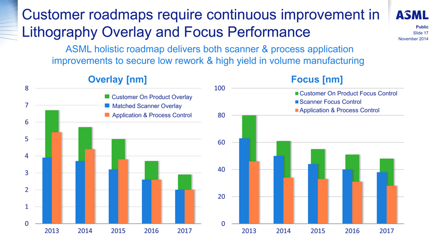
�
ASML
Public
Slide 17
November 2014
Customer roadmaps require continuous improvement in Lithography Overlay and Focus Performance
ASML holistic roadmap delivers both scanner�& process application improvements to secure low rework�& high yield in volume manufacturing
8
7
6
5
4
3
2
1
0
Overlay [nm]
Customer On Product Overlay
Matched Scanner Overlay
Application & Process Control
2013 2014 2015 2016 2017
100
80
60
40
20
0
Focus [nm]
Customer On Product Focus Control
Scanner Focus Control
Application & Process Control
2013 2014 2015 2016 2017
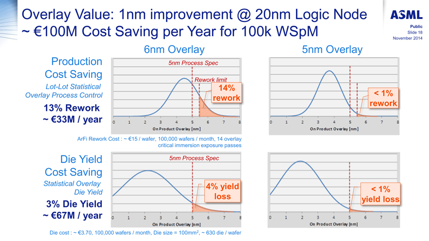
�
ASML
Public
Slide 18
November 2014
Overlay Value: 1nm improvement @ 20nm Logic Node
~ €100M Cost Saving per Year for 100k WSpM
6nm Overlay 5nm Overlay
Production 5nm Process Spec
Cost Saving
Rework limit
Lot-Lot Statistical 14%
Overlay Process Control rework < 1%
13% Rework rework
~ €33M / year 0 1 2 3 4 5 6 7 8 0 1 2 3 4 5 6 7 8
On Product Overlay [nm] On Product Overlay [nm]
ArFi Rework Cost : ~ €15 / wafer, 100,000 wafers / month, 14 overlay
critical immersion exposure passes
Die Yield 5nm Process Spec
Cost Saving
Statistical Overlay 4% yield < 1%
Die Yield
3% Die Yield loss yield loss
~ €67M / year 0 1 2 3 4 5 6 7 8 0 1 2 3 4 5 6 7 8
On Product Overlay [nm] On Product Overlay [nm]
Die cost : ~ €3.70, 100,000 wafers / month, Die size = 100mm2, ~ 630 die / wafer
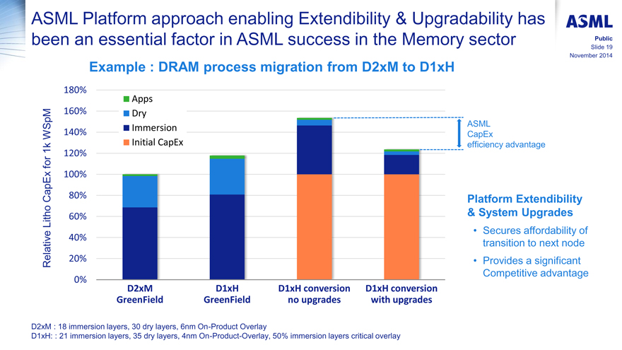
�
ASML
Public
Slide 19
November 2014
ASML Platform approach enabling Extendibility�& Upgradability has been an essential factor in ASML success in the Memory sector
Example : DRAM process migration from D2xM to D1xH
Relative Litho CapEx for 1k WSpM
180%
Apps
160% Dry
Immersion ASML
140% CapEx
Initial CapEx efficiency advantage
120%
100%
80% Platform Extendibility
60% & System Upgrades
Secures affordability of
40% transition to next node
20% Provides a significant
Competitive advantage
0%
D2xM D1xH D1xH conversion D1xH conversion
GreenField GreenField no upgrades with upgrades
D2xM : 18 immersion layers, 30 dry layers, 6nm On-Product Overlay
D1xH: : 21 immersion layers, 35 dry layers, 4nm On-Product-Overlay, 50% immersion layers critical overlay
�
ASML
Public
Slide 20
November 2014
Outline
Introduction
ASML value drivers
Market opportunity�& affordability
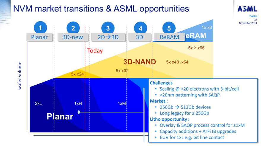
�
ASML
Public
21
November 2014
NVM market transitions�& ASML opportunities
wafer volume
12345
1x x8
Planar
3D-new
2D-->3D
3D
ReRAM
eRAM
Today
5x � x96
3D-NAND
5x x48~x64
5x x32
5x x24
2xL
1xH
1xM
Planar
Challenges
Scaling @ <20 electrons with 3-bit/cell
<20nm patterning with SAQP
Market :
256Gb --> 512Gb devices
Long legacy for � 256Gb
Litho opportunity :
Overlay�& SAQP process control for �1xM
Capacity additions + ArFi IB upgrades
EUV for 1xL e.g. bit line contact
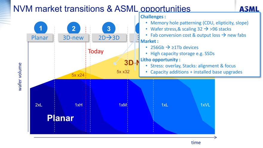
�
ASML
NVM market transitions�& ASML opportunities
wafer volume
123
Planar
3D-new
2D -> 3D
Today
3D-
5x x32
5x x24
2xL
1xH
1xM
Planar
Challenges :
Memory hole patterning (CDU, elipticity, slope)
Wafer stress,& scaling 32 -> >96 stacks
Fab conversion cost�& output loss -> new fabs
Market :
256Gb -> �1Tb devices
High capacity storage e.g. SSDs
Litho opportunity :
Stress: overlay, Stacks: alignment�& focus
Capacity additions + installed base upgrades
1xL
1xVL
time
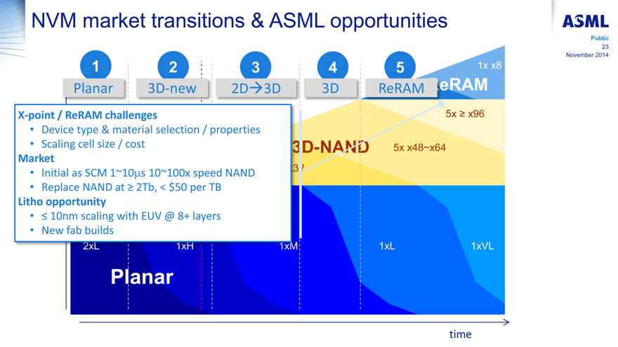
�
ASML
Public
23
November 2014
NVM market transitions�& ASML opportunities
12345
1x x8
Planar
3D-new
2D -> 3D
3D
ReRAM
eRAM
X-point / ReRAM challenges
Device type�& material selection / properties
Scaling cell size / cost
Market
Initial as SCM 1~10�s 10~100x speed NAND
Replace NAND at � 2Tb, < $50 per TB
Litho opportunity
� 10nm scaling with EUV @ 8+ layers
New fab builds
Planar
5x � x96
5x x48~x64
2xL
1xH
1xM
1xL
1xVL
time
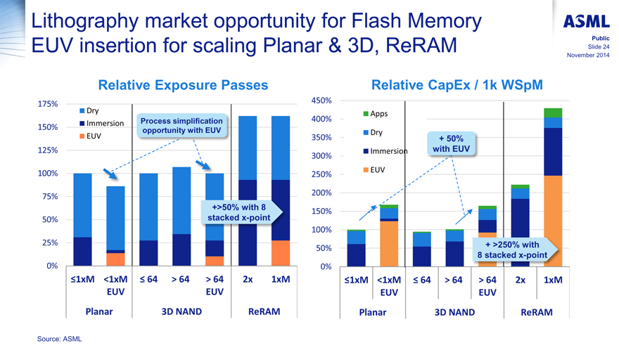
�
ASML
Public
Slide 24
November 2014
Lithography market opportunity for Flash Memory EUV insertion for scaling Planar�& 3D, ReRAM
Relative Exposure Passes
175% 150%
Dry
Immersion
EUV
Process simplification
opportunity with EUV
125%
100%
75%
+>50% with 8
50% stacked x-point
25%
0%
�1xM <1xM � 64 > 64 > 64 2x 1xM
EUV EUV
Planar 3D NAND ReRAM
Relative CapEx / 1k WSpM
450%
Apps
400%
Dry
350%
Immersion
+50% with EUV
300%
250% EUV
200%
150%
100%
50% + >250% with
8 stacked x-point
0%
�1xM <1xM �64 > 64 > 64 2x 1xM
EUV EUV
Planar 3D NAND ReRAM
Source: ASML
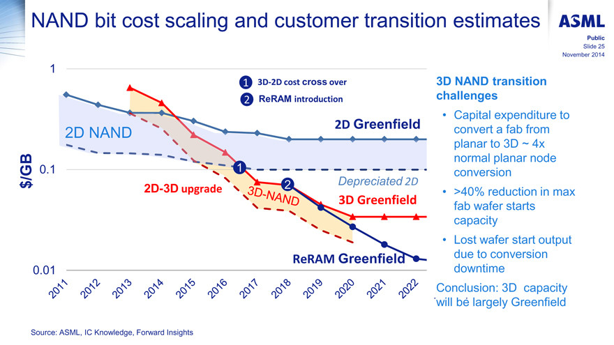
�
ASML
Public
Slide 25
November 2014
NAND bit cost scaling and customer transition estimates
$/GB
1
1 3D-2D cost cross over
2 ReRAM introduction
2D NAND 2D Greenfield
0.1 1
2D-3D upgrade 3D-NAND 2 Depreciated 2D
3D Greenfield
ReRAM Greenfield
0.01
2011
2012
2013
2014
2015
2016
2017
2018
2019
2020
2021
2022
3D NAND transition
challenges
Capital expenditure to convert a fab from planar to 3D ~ 4x normal planar node conversion
>40% reduction in max fab wafer starts capacity
Lost wafer start output due to conversion downtime
Conclusion: 3D capacity will be largely Greenfield
Source: ASML, IC Knowledge, Forward Insights
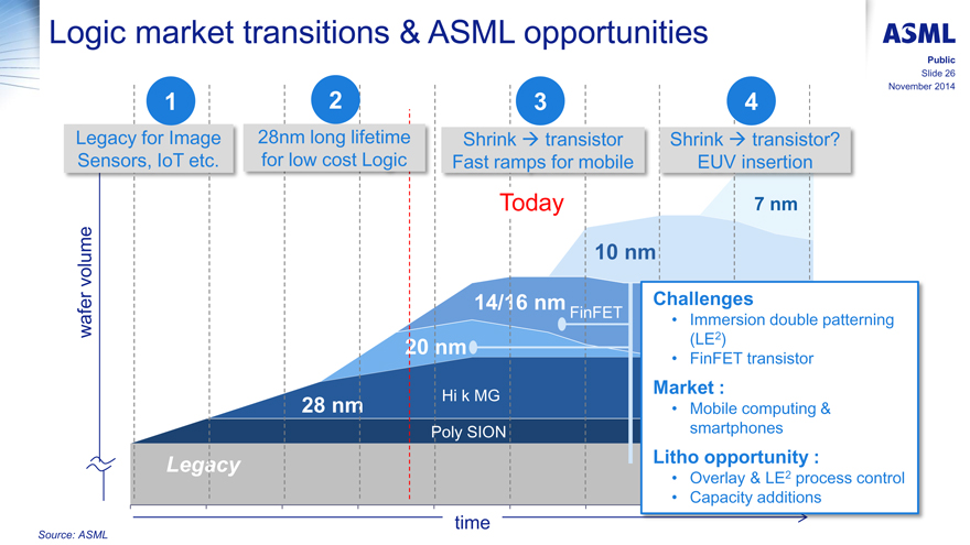
�
ASML
Public
Slide 26
November 2014
Logic market transitions�& ASML opportunities
wafer volume
1234
Legacy for Image 28nm long lifetime Shrink -> transistor Shrink -> transistor?
Sensors, IoT etc. for low cost Logic Fast ramps for mobile EUV insertion
Today 7 nm
10 nm
14/16 nm FinFET
20 nm
28 nm Hi k MG
Poly SION
Legacy
Challenges
Immersion double patterning (LE2)
FinFET transistor
Market :
Mobile computing�& smartphones
Litho opportunity :
Overlay�& LE2 process control
Capacity additions
time
Source: ASML
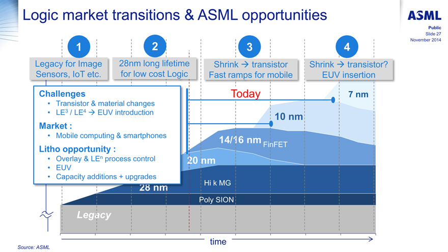
�
ASML
Public
Slide 27
November 2014
Logic market transitions�& ASML opportunities
1234
Legacy for Image 28nm long lifetime Shrink -> transistor Shrink -> transistor?
Sensors, IoT etc. for low cost Logic Fast ramps for mobile EUV insertion
Challenges
Transistor�& material changes
LE3 / LE4 -> EUV introduction
Market :
Mobile computing�& smartphones
Litho opportunity :
Overlay�& LEn process control
EUV
Capacity additions + upgrades
Today 7 nm
10 nm
14/16 nm FinFET
20 nm
Hi k MG
28nm
Poly SION
Legacy
time
Source: ASML
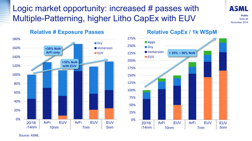
�
ASML
Public
Slide 28
November 2014
Logic market opportunity: increased # passes with Multiple-Patterning, higher Litho CapEx with EUV
Relative # Exposure Passes
180%
Dry
160% +30% NoN Immersion
ArFi only EUV
140%
+10% NoN
120% with EUV
100%
80%
60%
40%
20%
0%
20/16 ArFi EUV ArFi EUV EUV
/14nm 10nm 7nm 5nm
Relative CapEx / 1k WSpM
275%
250%
225% + 35% ~ 50% NoN
200%
175%
150%
125%
100%
75%
50%
25%
0%
Apps
Dry
Immersion
EUV
20/16 ArFi EUV ArFi EUV EUV
/14nm 10nm 7nm 5nm
Source: ASML
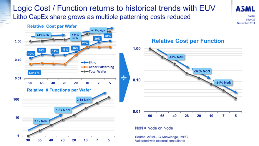
�
ASML
Public
Slide 29
November 2014
Logic Cost / Function returns to historical trends with EUV
Litho CapEx share grows as multiple patterning costs reduced
Relative Cost per Wafer
+17% NoN
+4% NoN +44% 31%
NoN 29%
1.00 20%
18% 15% 16%
14%
12%
0.10
Litho
Other Patterning
Litho % Total Wafer
0.01
90 65 40 28 20 10 7 5
Relative # Functions per Wafer
100 2.1x NoN
1.8x NoN
10
2.0x NoN
1
90 65 40 28 20 10 7 5
�
Relative Cost per Function
1.00
-45% NoN
-32% NoN
0.10
-41% NoN
0.01
90 65 40 28 20 10 7 5
NoN = Node on Node
Source: ASML, IC Knowledge, IMEC Validated with external consultants
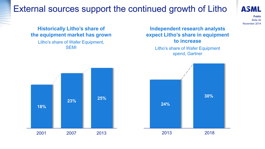
�
ASML
Public
Slide 30
November 2014
External sources support the continued growth of Litho
Historically Litho�s share of the equipment market has grown
Litho�s share of Wafer Equipment, SEMI
18%
23% 25%
2001 2007 2013
Independent research analysts expect Litho�s share in equipment to increase
Litho�s share of Wafer Equipment spend, Gartner
24%
30%
2013 2018
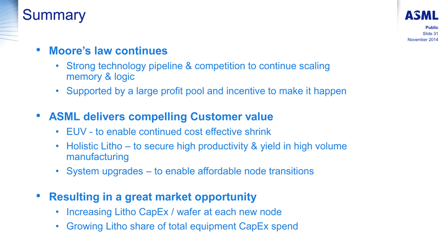
�
ASML
Public
Slide 31
November 2014
Summary
Moore�s law continues
Strong technology pipeline�& competition to continue scaling memory�& logic
Supported by a large profit pool and incentive to make it happen
ASML delivers compelling Customer value
EUV - to enable continued cost effective shrink
Holistic Litho � to secure high productivity�& yield in high volume manufacturing
System upgrades � to enable affordable node transitions
Resulting in a great market opportunity
Increasing Litho CapEx / wafer at each new node
Growing Litho share of total equipment CapEx spend

�
ASML
INVESTOR DAY
ASMLSMALLTALK2014
LONDON
Exhibit 99.8
�
�
ASML
Financial Model
Wolfgang Nickl
Executive Vice President�& Chief Financial Officer
24�November 2014
INVESTOR DAY
ASMLSMALLTALK2014
LONDON
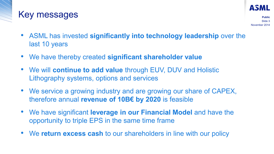
�
Key messages
ASML
Public
Slide 3
November 2014
ASML has invested significantly into technology leadership over the last 10 years
We have thereby created significant shareholder value
We will continue to add value through EUV, DUV and Holistic Lithography systems, options and services
We service a growing industry and are growing our share of CAPEX, therefore annual revenue of 10B€ by 2020 is feasible
We have significant leverage in our Financial Model and have the opportunity to triple EPS in the same time frame
We return excess cash to our shareholders in line with our policy
�
ASML
Public
Slide 4
November 2014
ASML created significant value over the last 10 years
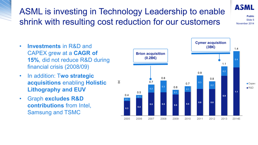
�
ASML is investing in Technology Leadership to enable shrink with resulting cost reduction for our customers
ASML
Public
Slide 5
November 2014
Investments in R&D and CAPEX grew at a CAGR of 15%, did not reduce R&D during financial crisis (2008/09)
In addition: Two strategic acquisitions enabling Holistic Lithography and EUV
Graph excludes R&D contributions from Intel, Samsung and TSMC
Cymer acquisition
(3B€)
Brion acquisition
(0.2B€)
B€
0.4
0.1
0.3
2005
0.5
0.1
0.4
2006
0.7
0.2
0.5
2007
0.8
0.3
0.5
2008
0.6
0.1
0.5
2009
0.7
0.1
0.5
2010
0.9
0.3
0.6
2011
0.8
0.2
0.6
2012
1.1
0.2
0.9
2013
1.4
0.4
1.1
2014E
Capex
R&D
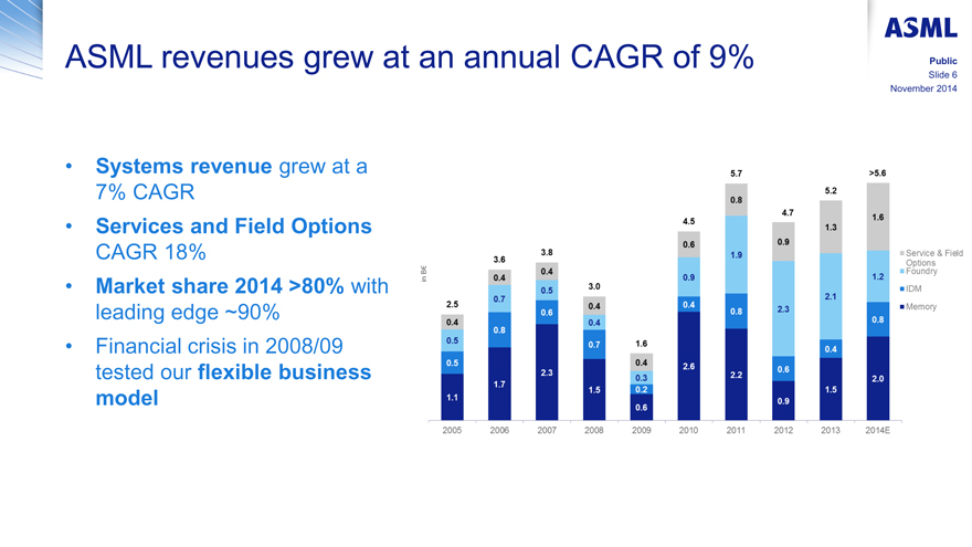
�
ASML revenues grew at an annual CAGR of 9%
ASML
Public
Slide 6
November 2014
Systems revenue grew at a 7% CAGR
Services and Field Options
CAGR 18%
Market share 2014 >80% with leading edge ~90%
Financial crisis in 2008/09 tested our flexible business model
in B€
2.5 0.4 0.5 0.5 1.1 2005
3.6 0.4 0.7 0.8 1.7 2006
3.8 0.4 0.5 0.6 2.3 2007
3.0 0.4 0.4 0.7 1.5 2008
1.6 0.4 0.3 0.2 0.6 2009
4.5 0.6 0.9 0.4 2.6 2010
5.7 0.8 1.9 0.8 2.2 2011
4.7 0.9 2.3 0.6 0.9 2012
5.2 1.3 2.1 0.4 1.5 2013
>5.6 1.6 1.2 0.8 2.0 2014E
Service�& Field
Options
Foundry
IDM
Memory
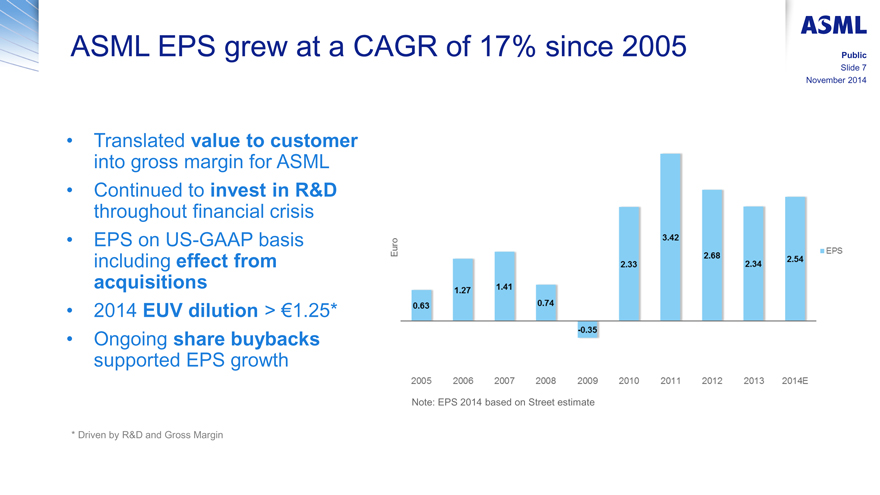
�
ASML EPS grew at a CAGR of 17% since 2005
ASML
Public
Slide 7
November 2014
Translated value to customer into gross margin for ASML
Continued to invest in R&D throughout financial crisis
EPS on US-GAAP basis including effect from acquisitions
2014 EUV dilution > €1.25*
Ongoing share buybacks supported EPS growth
Euro
0.63 1.27 1.41 0.74 -0.35 2.33 3.42 2.68 2.34 2.54 EPS
2005 2006 2007 2008 2009 2010 2011 2012 2013 2014E
Note: EPS 2014 based on Street estimate
* Driven by R&D and Gross Margin
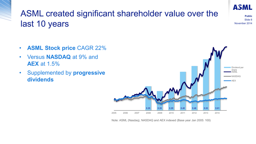
�
ASML created significant shareholder value over the last 10 years
ASML
Public
Slide 8
November 2014
ASML Stock price CAGR 22%
Versus NASDAQ at 9% and AEX at 1.5%
Supplemented by progressive dividends
Dividend per share
ASML
NASDAQ
AEX
0.25 0.20 0.20 0.40 0.46 0.53 0.61
2005 2006 2007 2008 2009 2010 2011 2012 2013 2014
Note: ASML (Nasdaq), NASDAQ and AEX indexed (Base year Jan 2005: 100)
�
ASML
Public
Slide 9
November 2014
We service a growing industry and annual revenue of 10B€ is feasible by 2020
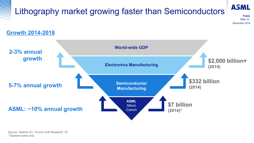
�
Lithography market growing faster than Semiconductors
ASML
Public
Slide 10
November 2014
Growth 2014-2018
2-3% annual growth 5-7% annual growth ASML: ~10% annual growth
World-wide GDP Electronics Manufacturing Semiconductor Manufacturing ASML Nikon Canon
$2,000 billion+ (2014) $332 billion (2014) $7 billion (2014)*
Source: Gartner Q1 �14 and VLSI Research �14
* Systems sales only
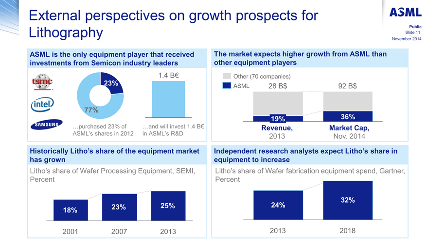
�
External perspectives on growth prospects for Lithography
ASML
Public
Slide 11
November 2014
ASML is the only equipment player that received investments from Semicon industry leaders
tsmc intel SAMSUNG
23% 77% �purchased 23% of ASML�s shares in 2012
1.4 B€ �and will invest 1.4 B€ in ASML�s R&D
The market expects higher growth from ASML than other equipment players
Other (70 companies)
ASML 28 B$ 92 B$
19% 36%
Revenue, Market Cap,
2013 Nov. 2014
Historically Litho�s share of the equipment market has grown
Litho�s share of Wafer Processing Equipment, SEMI, Percent
18% 23% 25%
2001 2007 2013
Independent research analysts expect Litho�s share in equipment to increase
Litho�s share of Wafer fabrication equipment spend, Gartner, Percent
24% 32%
2013 2018
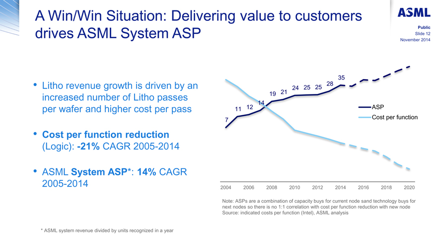
�
A Win/Win Situation: Delivering value to customers drives ASML System ASP ASML
Public
Slide 12
November 2014
Litho revenue growth is driven by an increased number of Litho passes per wafer and higher cost per pass
Cost per function reduction
(Logic): -21% CAGR 2005-2014
ASML System ASP*: 14% CAGR 2005-2014
7 11 12 14 19 21 24 25 25 28 35
ASP
Cost per function
2004 2006 2008 2010 2012 2014 2016 2018 2020
Note: ASPs are a combination of capacity buys for current node sand technology buys for next nodes so there is no 1:1 correlation with cost per function reduction with new node
Source: indicated costs per function (Intel), ASML analysis
* ASML system revenue divided by units recognized in a year
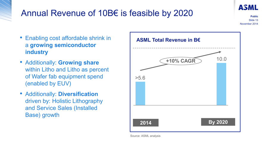
�
Annual Revenue of 10B€ is feasible by 2020 ASML
Public
Slide 13
November 2014
Enabling cost affordable shrink in a growing semiconductor industry
Additionally: Growing share within Litho and Litho as percent of Wafer fab equipment spend (enabled by EUV)
Additionally: Diversification driven by: Holistic Lithography and Service Sales (Installed Base) growth
ASML Total Revenue in B€
+10% CAGR 10.0
>5.6
2014 By 2020
Source: ASML analysis
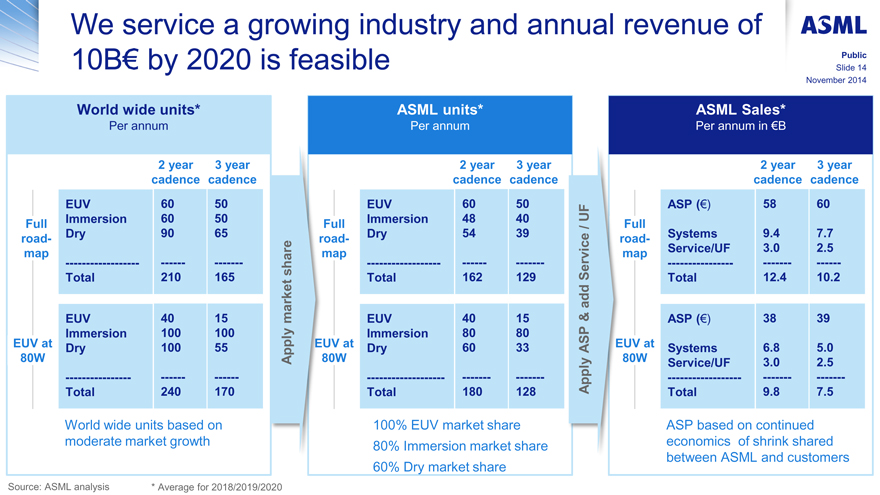
�
We service a growing industry and annual revenue of 10B€ by 2020 is feasible ASML
Public
Slide 14
November 2014
World wide units* ASML units* ASML Sales*
Per annum Per annum Per annum in €B
2 year 3 year 2 year 3 year 2 year 3 year
cadence cadence cadence cadence cadence cadence
Full road-map EUV 60 50 Apply market share Full road-map EUV 60 50 Apply ASP & add Service /UF Full road-map ASP (€) 58 60
Immersion 60 50 Immersion 48 40
Dry 90 65 Dry 54 39 Systems 9.4 7.7 Service/UF 3.0 2.5
Total 210 165 Total 162 129 Total 12.4 10.2
EUV at 80W EUV 40 15 EUV at 80W EUV 40 15 EUV at 80W ASP (€) 38 39
Immersion 100 100 Immersion 80 80
Dry 100 55 Dry 60 33 Systems 6.8 5.0 Service/UF 3.0 2.5
Total 240 170 Total 180 128 Total 9.8 7.5
World wide units based on moderate market growth
100% EUV market share
80% Immersion market share
60% Dry market share
ASP based on continued economics of shrink shared between ASML and customers
Source: ASML analysis * Average for 2018/2019/2020
�
ASML
Public
Slide 15
November 2014
We have significant leverage in our Financial Model and significant upside potential to EPS
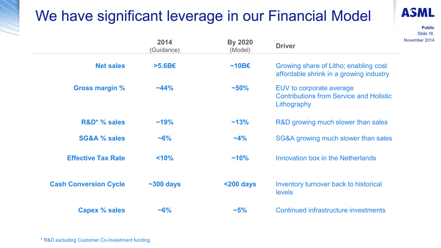
�
We have significant leverage in our Financial Model
ASML
Public
Slide 16
November 2014
Net sales
Gross margin %
R&D* % sales
SG&A % sales
Effective Tax Rate
Cash Conversion Cycle
Capex % sales
2014
(Guidance)
>5.6B€
~44%
~19%
~6%
<10%
~300 days
~6%
By 2020
(Model)
~10B€
~50%
~13%
~4%
~10%
<200 days
~5%
Driver
Growing share of Litho; enabling cost affordable shrink in a growing industry
EUV to corporate average Contributions from Service and Holistic Lithography
R&D growing much slower than sales
SG&A growing much slower than sales
Innovation box in the Netherlands
Inventory turnover back to historical levels
Continued infrastructure investments
* R&D excluding Customer Co-Investment funding
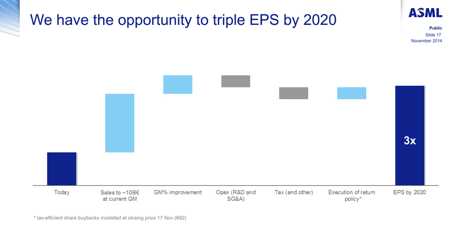
�
We have the opportunity to triple EPS by 2020
ASML
Public
Slide 17
November 2014
3x
Today
Sales to ~10B€ at current GM
GM% improvement
Opex (R&D and SG&A)
Tax (and other)
Execution of return policy*
EPS by 2020
* tax-efficient share buybacks modelled at closing price 17 Nov (€82)
�
ASML
Public
Slide 18
November 2014
We return excess cash to our shareholders in line with our policy
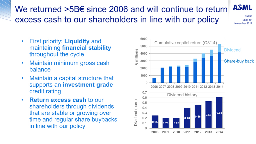
�
We returned >5B€ since 2006 and will continue to return excess cash to our shareholders in line with our policy
ASML
Public
Slide 19
November 2014
First priority: Liquidity and maintaining financial stability throughout the cycle
Maintain minimum gross cash balance
Maintain a capital structure that supports an investment grade credit rating
Return excess cash to our shareholders through dividends that are stable or growing over time and regular share buybacks in line with our policy
€ millions
6000
5000
4000
3000
2000
1000
0
Cumulative capital return (Q3�14)
Dividend
Share-buy back
2006 2007 2008 2009 2010 2011 2012 2013 2014
Dividend (euro)
0.7 0.6 0.5 0.4 0.3 0.2 0.1 0
Dividend history
0.25 0.20 0.20 0.40 0.46 0.53 0.61
2008 2009 2010 2011 2012 2013 2014

�
ASML
Investor Day
ASMLSMALLTALK2014
LONDON
Exhibit 99.9
| � |

ASML
Closing remarks
Peter Wennink
President�& Chief Executive Officer
24�November 2014
INVESTOR DAY
ASMLSMALLTALK2014
LONDON
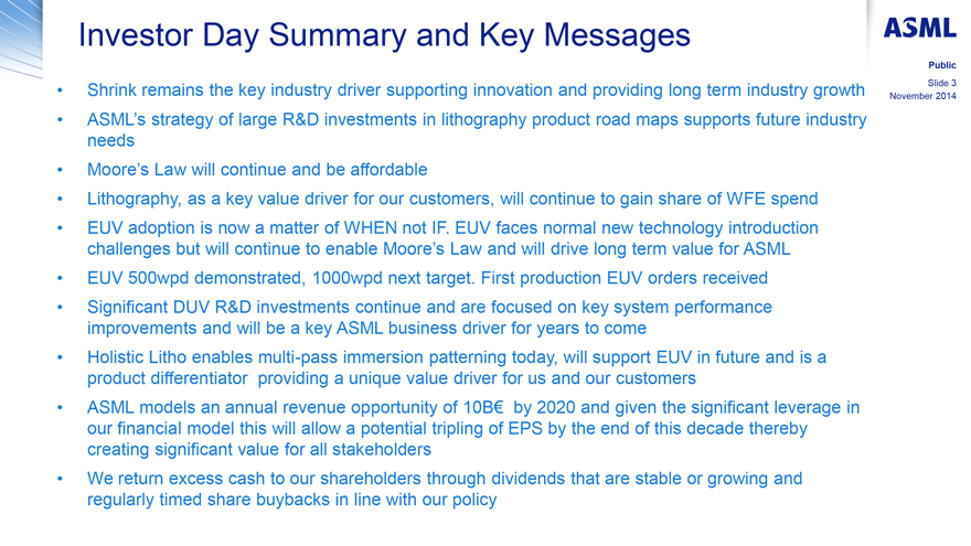
�
Investor Day Summary and Key Messages ASML
Public
Slide 3
November 2014
Shrink remains the key industry driver supporting innovation and providing long term industry growth
ASML�s strategy of large R&D investments in lithography product road maps supports future industry needs
Moore�s Law will continue and be affordable
Lithography, as a key value driver for our customers, will continue to gain share of WFE spend
EUV adoption is now a matter of WHEN not IF. EUV faces normal new technology introduction challenges but will continue to enable Moore�s Law and will drive long term value for ASML
EUV 500wpd demonstrated, 1000wpd next target. First production EUV orders received
Significant DUV R&D investments continue and are focused on key system performance improvements and will be a key ASML business driver for years to come
Holistic Litho enables multi-pass immersion patterning today, will support EUV in future and is a product differentiator providing a unique value driver for us and our customers
ASML models an annual revenue opportunity of 10B€ by 2020 and given the significant leverage in our financial model this will allow a potential tripling of EPS by the end of this decade thereby creating significant value for all stakeholders
We return excess cash to our shareholders through dividends that are stable or growing and regularly timed share buybacks in line with our policy

�
ASML
Investor day
ASMLSMALLTALK2014
LONDON
Serious News for Serious Traders! Try StreetInsider.com Premium Free!
You May Also Be Interested In
- Argus on ASML Inc. (ASML): 'Remaining cautious on 2024'
- ROSEN, NATIONAL TRIAL LAWYERS, Encourages Northern Genesis Acquisition Corp. n/k/a The Lion Electric Company Investors to Secure Counsel Before Important Deadline in Securities Class Action – NGA
- TotalEnergies BWF Thomas & Uber Cup Finals 2024 to Kick Off in Chengdu
Create E-mail Alert Related Categories
SEC FilingsSign up for StreetInsider Free!
Receive full access to all new and archived articles, unlimited portfolio tracking, e-mail alerts, custom newswires and RSS feeds - and more!